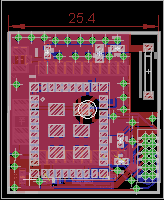
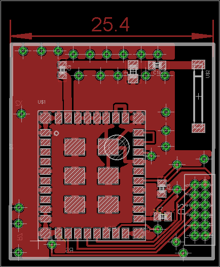
Hi,
Somebody please review my schematics before I give it for manufacturing.
I have attached the design file here.
Thanking in advance,
Swarika Jain
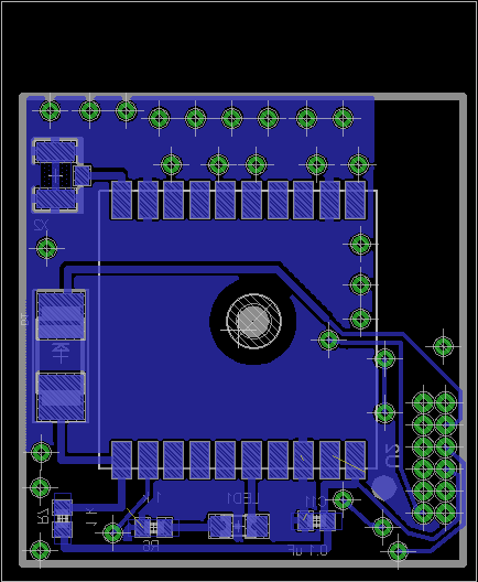
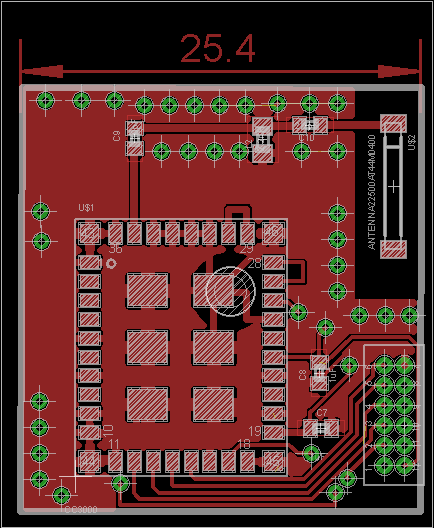
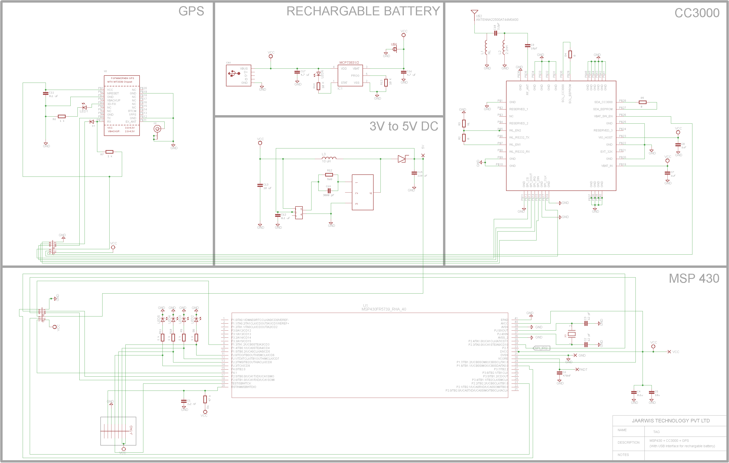
Hi,
Somebody please review my schematics before I give it for manufacturing.
I have attached the design file here.
Thanking in advance,
Swarika Jain