This thread has been locked.

If you have a related question, please click the "Ask a related question" button in the top right corner. The newly created question will be automatically linked to this question.

PCB Design clarity required to use the 2.4GHz Antenna

Other Parts Discussed in Thread: CC3200, CC3100

I am designing a Hardware using CC3200.

I am following CC3100 and CC3200 SimpleLink™ Wi-Fi® and IoT Solution Layout Guidelines, User's Manual.

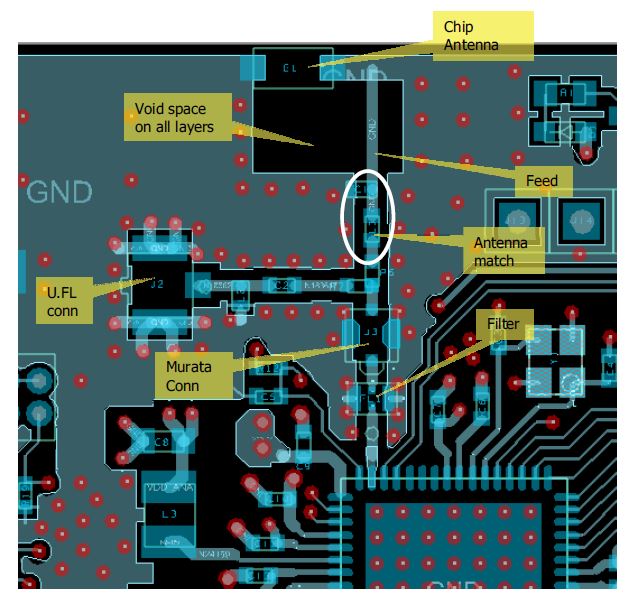
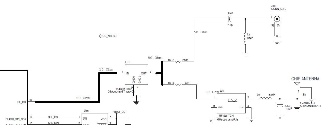
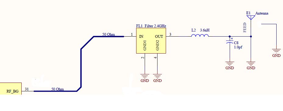
According to this attached Image in User's Manual, (Figure 7. RF Section Layout); I am in doubt that both the pads of the chip antenna are ground, as the feed is directly connected to the ground.

How will it work?, Please clarify this method. 

  • Rushi,

    That`s the beauty of high frequency design. You cannot look at the feed as a DC signal going straight to ground!

    At 2.4 GHz the feed line is an inductor connected to ground (used for matching) along with a feed to the λ/2 monopole chip antenna. This ``free`` shunt inductor along with the antenna match components and of course the ground plane cutouts all play a role in determining the resonance of the chip antenna. Without being on resonance there will be significant radiated power loss.

    An RF network analyzer with the final product assembly in free space should be used to select the antenna match components for targeting the resonance frequency and minimizing transmission line return loss.

  • Lotus,

    That's so Cool. Thank you for Reply. I got your explanation but as I can see in the reference schematics of the CC3200 Launchpad, there is one DNP resistor after the filter, so "free" shunt inductor L8 will not play any role.

    In reference design one series inductor L9 is connected after the switch, which is a part of matching circuit, I have edited the circuit as follows as I don't need the UFL connector and a RF switch, As you would be knowing that RF_BG is CC3200's 31st pin, which I have connected as follows. Please suggest the corrections needed. would it work correctly? 

    Best Regards,

    Rushi Gajjar.

  • Hi Rushi,

    What I meant by ``free`` inductor is the antenna feed line going to the ground plane. That is a small value inductor for matching the chip antenna. It is not a part but a short length trace on the PCB. For that matter a properly fixed and matched defined length of wire inside the enclosure can act as an antenna of better efficiency and lower cost than the ceramic chip component but does require more space.

    I can only assume that if you follow the same layout as TI has with the same PCB substrate material and no extra loading effects around the antenna from an enclosure, battery, etc. then the matching elements suggested should be good enough. Any deviation would require a re-match of the reference antenna. Removing the u.fl path and RF switch is fine as long as the match TI chose is of 50 ohm to the RF switch reference plane which typically is the case. Make sure your feed line is of 50 ohm characteristic impedance.

  • Ohh, yeah, Sorry for misinterpretation, I would be using the ceramic chip component as suggested by TI Reference design,  I would make sure for the 50ohm characteristic Independence during PCB design.


    Can you explain more about the statement given by you "An RF network analyzer with the final product assembly in free space should be used to select the antenna match components for targeting the resonance frequency and minimizing transmission line return loss."

    Thanks.

  • In order to achieve the best conversion efficiency from the radiated to conducted medium the antenna resonating element must be tuned to the right frequency (i.e. 2400-2484 MHz in this case) and must be matched to the right impedance (i.e. 50 ohm in this case). Tuning is required for adjusting the resonating element`s frequency to the signal of interest and matching for maximal power transfer between CC3200 and the resonating element. The antenna has to be evaluated as a final product configuration in a typical use environment because any other dielectric or conductive objects near the antenna will `load` it and move these tuned/matched points.

    Tuning and matching therefore has to happen at the final product stage for optimal radiated performance. An RF network analyzer is used for this purpose. You can easily double your over-the-air link distance or almost halve your DC power supply consumption by doing a proper antenna design vs. blindly following a reference design.

  • I got your point Lotus, I will surely take care of antenna matching circuit guidelines to design the board, Thank you for your valuable time.

    Best Regards,

    Rushi Gajjar.