This thread has been locked.

If you have a related question, please click the "Ask a related question" button in the top right corner. The newly created question will be automatically linked to this question.

cc3100 nxp lpc1769

Other Parts Discussed in Thread: CC3100, UNIFLASH

Hi,

I have designed a small cc3100 board (ca. 40 x 20mm) with spi connection to a lpc1769 board.he

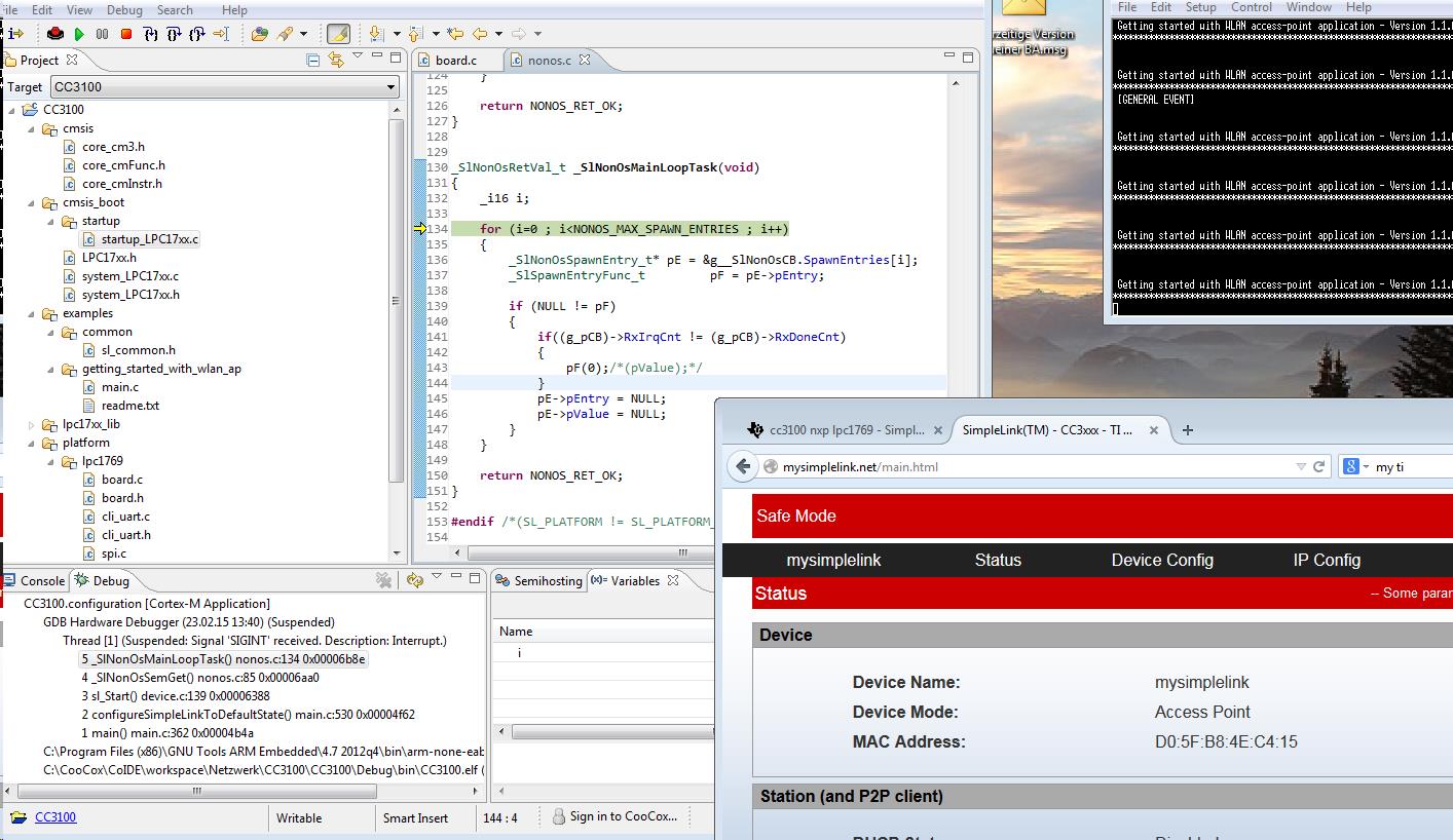
I have downloaded the example "getting started with ap" and there is no problem to access the website "mysimplelink.net2 in my browser:-)

But in my  serial terminal i have only reveived  the first line of the message "Getting started with station - Version 1.1.0"

I have also tried other examples  like "getting started with station"  with the same result. The Signals nHIB  Hostintr and ForceAP are correct (measured via oszilliscope and connected to my lpc1769 board)

thank you for your help

Otto Parzhuber

Munich University of Applied Sciences

  • Hi Otto,

    Can you please share few more details?
    1. Is your application able to initialize the networking sub system (sl_Start() function call)?
    2. Are you running the application in debug mode? If yes can you please share the exact location where the application is getting stuck?
    3. Did you try running the examples ported on LPC1769 with CC3100 BP.

    Regards,
    Ankur
  • Hi Ankur,

    thank you for your quick reply,

    This is a screenshot with debugger, serial console and Website:

    The application never leaves sl_Start().

    I Don't have connected my bp Hardware to my lpc1769 board yet.

    Thanks

    Otto Parzhuber

  • Hi Otto,

    I will suggest you to first test the ported solution on CC3100 BP + LPC board.
    It can also be a porting issue. Please make sure you are following the guidelines for the porting the solution on other platform. processors.wiki.ti.com/.../CC31xx_Host_Interface

    Regards,
    Ankur
  • Hi Ankur,

    i have tested my LPC-Board on CC3100 BP and I could successfully run the examples in the sdk examples folder.

    This is the output of the serial console after running the program on my CC3100 hardware. I have included outputs on spi read and spi write

     Getting started with WLAN access-point application - Version 1.1.0
    *******************************************************************************
    Wr: 65, 87, 78, 56
    Rd:  bc, dc, cd, ab
    Rd:  8, 0, 8, 0
    Rd:  0, 0, 0, 0
    Rd:  33, 33, 33, 33
    Wr: 65, 87, 78, 56
    Rd:  bd, dc, cd, ab
    Rd:  78, 0, 8, 0
    Rd:  38, 0, 0, 0
    Rd:  b3, 6, 33, 33
     [GENERAL EVENT]
    Wr: 65, 87, 78, 56
    Rd:  be, dc, cd, ab
    Rd:  25, 18, 10, 0
    Rd:  38, 0, 0, 0
    Rd:  1, 1, a8, c0
    Wr: 21, 43, 34, 12
    Wr: b4, 8c, 4, 0
    Wr: 0, a, 0, 10
    Wr: 65, 87, 78, 56
    Rd:  bf, dc, cd, ab
    Rd:  b4, c, 8, 0
    Rd:  38, 0, 0, 0
    Rd:  0, 0, 1, 1
    Wr: 21, 43, 34, 12
    Wr: 73, 84, 4, 0
    Wr: ff, 0, 0, 0
    Wr: 65, 87, 78, 56
    Rd:  bc, dc, cd, ab
    Rd:  73, 4, 8, 0
    Rd:  38, 0, 0, 0
    Rd:  0, 0, 1, 1
    Wr: 65, 87, 78, 56
    Rd:  bd, dc, cd, ab
    Rd:  73, 0, 8, 0
    Rd:  38, 0, 0, 0
    Rd:  0, 0, 6, b3
    Wr: 65, 87, 78, 56
    Rd:  bc, dc, cd, ab
    Rd:  8, 0, 8, 0
    Rd:  0, 0, 0, 0
    Rd:  33, 33, 33, 33
    Wr: 65, 87, 78, 56
    Rd:  bd, dc, cd, ab
    Rd:  78, 0, 8, 0
    Rd:  38, 0, 0, 0
    Rd:  b3, 6, 33, 33
     [GENERAL EVENT]
     Failed to configure the device in its default state

    Do you have an advice what could be wrong?

    Thank you

    Otto

  • Hi Otto,

    The interface communication between CC3100 and NXP looks to be fine but the application is failing. Can you please check and share the error return value by host driver function.

    Regards,
    Ankur
  • Hi Ankur,

    thnak you for your help. Following is an output of my console with returns of the device driver.

     Getting started with WLAN access-point application - Version 1.1.0
    *******************************************************************************
     [GENERAL EVENT]
    sl_Start: 2
    sl_WlanSetMod: 0
    sl_Stop: 0
     [GENERAL EVENT]
    sl_Start: 2
     Failed to configure the device in its default state

    In your Docs I have found the corresponding enum for the sl_Start return value:

    ROLE_AP_ERR (Failure to load MAC/PHY in AP role)

    Until now i haven't found any hardware error in my design.

    Thank you

    Otto

  • Hi Ankur,

    meanhwile I have measured a few voltages during start up of the program. I have measured strange voltages VDD_PA, VDD_PLL, VDD_RAM, DIG_CC, PA_SWP, PA_SWN and VDD_ANA. The VDD (3V3) has got constantly 3V3 with a small ripple.

    Probably its a hardware issue, but i don't know whats wrong on my design.

    CC3100 Fehlerprot_oszi.pdf

    Thank you

    Otto

  • Hi Otto,

    I am not able to see the images in above post.

    I have few question:
    How are you powering your board? How much current can be sourced by supply?
    Did you formatted and updated the service pack on the device using uniflash?

    Regards,
    Ankur
  • Hi Ankur
    I have included a pdf now....Your answer was too fast.

    I didn't format and update the service pack...but I think its a hardware failure.

    Updated pdf with all relevant voltages:5428.CC3100 Fehlerprot_oszi.pdf

    The two oscillators are working.

    Thank you
    Otto

  • Otto,

    Every new device + serial flash need's to be formatted and the service pack should be updated. This is required for the device to create its file system on the serial flash.
    This may be the cause of the above behaviour.

    Also please share the current rating for the CC3100 power source on your board.

    Regards,
    Ankur
  • Hi Ankur,

    meanwhile I have formatted the serial flash and have updated the device with a new servicepack.

    For testing I have connected the cc3100 board to a 5A powersupply. The board draws about 60 mA, measured with a simple multimeter.

    The result is the same as described in my last post.

    I have inluded 3 PDF Files:

    1) The measured voltages8875.CC3100 Fehlerprot_oszi.pdfCC3100BoardPhotos.pdfCC3100.PDF

    2) Schematic and PCB

    3) Photos of the Board.

    The main difference to the reference design are a few not included 100nF blocking Cs. (Components are placed on Top- and BottomLayer, SignalLayer1 is GND and SignalLayer2 is connected to the different Voltages (3V3, VDD_DIG_CC, VDD_PA and so on).The UART interface I have temporary connected with isolated wire to a ftdi chip.

    Thank you

    Otto

  • Hi Ankur,
    can you tell me which of the voltages are depending on VDD_ANA?
    Thank you
    Otto
  • Hi Otto,

    Apologies for the delayed response.

    Your layout is very much deviating from our reference design. We will suggest you to keep the same layout.
    Also we can see some capacitors missing from schematics and the inductors chosen are of very low current capacity.

    May be you can consider using the Module.

    Regards,
    Ankur
  • Thank you Ankur,

    meanwhile I have designed a new Board with nearly the same placement of components and same routing as your refernece design.

    When the board is assembled I will tell you the result.

    Regards

    Otto

  • Hi Otto,

    Thanks for the update.
    I am closing this thread, for follow up queries please open a new thread and a link to this one for reference.

    Regards,
    Ankur