


Background
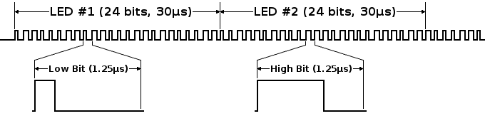
I'm working on a port of OctoWS2811 for the CC3200 to control multiple LED strips with minimal processor overhead (i.e. DMA). The basic idea OctoWS2811 uses is to generate two synced 800 kHz PWM waveforms, essentially creating 3 timing points in a 800 kHz cycle: 1 for both rising edges, 1 for the first falling edge (T0H), and 1 for the second falling edge (T1H). Each timing point should trigger a DMA request to move pre-formatted data from memory into the bit-banded GPIO register. The two ways to implement this on the CC3200 DMA that I see are: have 2 DMA requests, with one PWM timer triggering on both edges; have 3 DMA requests: both PWM set to request on falling edge, and the PWM wave jumpered to another pin which DMA request on rising edge.
While there are solutions here, all of them seem to require 100% processor usage while outputting data, only able to output 1 strip at once, or require a lot of data conversion to convert from standard RGB structs to data output to the WS2812, so I decided to try to port OctoWS2811 (which was built for a Freescale Cortex-M4 MCU).
 (from Paul Stoffregen's website)
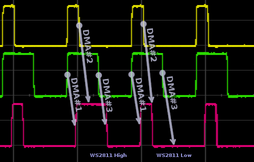
What it should look like (first 2 channels = PWM 1 & 2, 3rd = output):
WHAT WORKS:
I have been able to generate the PWM waveforms (verified on an oscilloscope), and can write data to the GPIO register using DMA triggered by PWM.
STRUGGLING WITH:
PWM DMA Request triggering source.
I used this E2E question to generate a DMA request, testing it by DMA'ing data to toggle GPIO pins every DMA request. However, there was a 200 ns delay between a rising PWM edge and the GPIO toggle. (I don't have the waveform saved, but it might have only registered every two PWM cycles as well).
Further, when changing the edge detection (TimerControlEvent(TIMERA3_BASE,TIMER_B,TIMER_EVENT_POS_EDGE);) from posedge to negedge to both edges, it seemed to toggle the GPIO at the same time regardless, so I don't know what the PWM DMA request is sourced from (timer match/load, or positive edge, negative edge, or constant regardless of settings)?
Ideally, I would like it to trigger a DMA request on both edges of a T1H waveform (spaced ~700 ns apart). Barring that, at least consistently trigger on negative edge of both PWM signals
Does a PWM DMA event just generate one DMA request (not burst). That is, on each PWM edge match, only 1 byte should be sent if the channel is DMA_ARB_1 and size = 8bits?
GPIO DMA Interrupt Source
What generates a DMA Request from GPIO? Does it occur if an interrupt (i.e. rising edge on Pin 1) would occur? How many DMA requests are generated by a single pin event (is the DMA request continually sent if the interrupt is level-sensitive and only sent once if the interrupt is edge-triggered)?
GPIO Pin Interrupt & DMA ISR
Is there any way to attach a DMA Done ISR just to the DMA Done interrupt, and not the generic pins? The problem comes when a DMA request is sent by repeating signal (i.e. square wave). If the DMA requests on a posedge, then the CC3200 will interrupt on that posedge (see above question), because the DMA DONE & PIN INTERRUPT are attached to the same RIS (Raw Interrupt Status) register. So this requires checking the DMA DONE bit to see if the DMA transfer has actually finished?? Which is fine, except that this ISR is called at about 800 kHz for the WS2812, so the MCU spends most time entering/exiting the ISR triggered by each rising edge from the 800 kHz PWM signal.
GPIO DMA Request Failure
For some reason, even with setting up the DMA transfer & GPIO trigger, it wouldn't send the data to the output GPIO register. This same method worked fine for the PWM DMA requests, I could show those toggling the GPIO pins which demonstrated working DMA transfers
Pseudocode (from a program just to test GPIO DMA transfers using 800 kHz input from Waveform generator)
//Not shown: set up GPIO 28 (CC3200 chip pin 18) as input, and a different GPIO port as output
GPIOIntTypeSet(GPIOA3_BASE, GPIO_PIN_4, GPIO_RISING_EDGE);

UDMAInit(); // from SDK Common Examples' udma_if.h

uDMAChannelDisable(UDMA_CH7_GPIOA3);
uDMAChannelControlSet(UDMA_CH7_GPIOA3, UDMA_SIZE_8 | UDMA_SRC_INC_8 | UDMA_DST_INC_NONE | UDMA_ARB_1);
//Not shown: disable attributes AltSelect, Useburst (even though enabled in SetupTransfer from udma_if.c), and ReqMask
//Not shown: enable attribute high priority

GPIODMATriggerEnable(GPIOA3_BASE); //I think this should now send one DMA request per rising edge of GPIO 28.

//Not shown: Use SetupTransfer to start a PingPong transfer from a buffer filled w/ alternating 0xFF & 0x00 to the GPIO output pins (correctly bit-banded address)
//Enable DMA Channel 7

GPIOIntRegister(GPIOA3_BASE, gpioISR); //ISR not shown, basically checks if DMA actually done (b/c triggers on posedge of GPIO28 too), and keeps track of number of transfers, renews transfer if necessary, and stops when done.

//set GPIO A3 to generate interrupt on Pin 4 (GPIO 28) posedge, and DMA Done
HWREG(GPIOA3_BASE + GPIO_O_GPIO_IM) |= GPIO_INT_DMA | GPIO_INT_PIN_4;


//If GPIO is fed with a 800 kHz square wave, should trigger DMA transfer now.
Preserve DMA timing even with DMA startup latency
As mentioned above, the latency between a PWM DMA request & GPIO output seems to be about 200ns. However, I've seen waveforms that essentially strobe high for ~100 ns, then reset to 0 (timing should be ~300 for T0H transfer). I assume this is due to some DMA startup latency in the uDMA peripheral, which then processes the second request very quickly. Is there some way to preserve the relative timing of these two transfers?
If oscilloscope screenshots would be useful for any of these questions, let me know. I didn't have a USB drive to copy screenshots at the time.
