This thread has been locked.

If you have a related question, please click the "Ask a related question" button in the top right corner. The newly created question will be automatically linked to this question.

LAUNCHCC3220MODASF: How to connect the emulator section of the LAUNCHCC3220MODASF board to a CC3220MODASF module

Part Number: LAUNCHCC3220MODASF

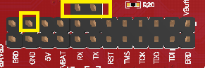
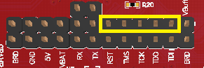
I've got a a CC3220MODASF launchpad board (LAUNCHCC3220MODASF).  I've also designed a scaled down PCB with the CC3220MODASF module, flash IC, voltage regulator, jumpers and breakout pins for internal development of hardware designs.  

If I want to use the emulator section on the LAUNCHCC3220MODASF board to program and debug the scaled down board I designed, how do I go about doing that?  How do I attach my schematic?

  • SGW_Dave,

    First you want to remove all the jumpers from the power, UART, and JTAG headers (BRD, GND, 5V, VBAT, RX, TX, RST, TMS, TCK, etc.) on the LaunchPad. Then you want to make sure have a common ground by connecting the ground pins from each board. 

    To program, connect the top row pins of the UART headers (shown below) to the corresponding UART pins on your custom PCB. In other words, the UART pin on the left marked RX and the UART pin on the right marked TX must be connected to pin 47 and pin 46, respectively. 

    To debug, you can use J4 (XDS110 OUT) OR the top row pins of the JTAG headers (shown below). 

    Connect TMS, TCK, TDO, TDI to pins 22, 21, 18, and 12, respectively. Connect RST to your reset circuit.

    Please note that you need a 100k pull down resistor on pin 21.

    Hope this helps,

    Seong

  • That worked.  Thank you!

  • Glad you got it working!

    -Seong
  • I completed a board layout of our design using the CC3220MODASF12 part.  I'm having problems getting it to program using the LAUNCHCC3220MODASF emulator/programmer side of the board.  I've connected the GND, TX,RX, RST, TMS, TCK, TDO, TDI on my new board as covered in the previous forum post.  I get a timeout error with UniFlash.  Do you have any idea on what could be causing the problem?  Attached is my schematic.  

    Items corrected on the PCB:

    1.  Added a 100K resistor from pin 21 (JTAG_TCK) of the CC3220 module to ground

    2.  Added a 100K resistor from ppin 23 (RESET) of the CC3220 module to +3.3VDC

    3.  Odd and even sides are of P1 and P2 are reversed.  I'm not sure how that happen since I used the same part in the TI Altium project for this board.  I made an adapter to correct this problem.

    Question(s):

    Do I need a reset circuit for this module or is it handle internally?

    Smart Base V2.00.pdf

  • Dave,

    Pin 23 is SOP2, not the reset pin.

    Have you seen the hardware design checklist? If not, please use and follow the checklist for the CC3220MOD, which can be downloaded here: processors.wiki.ti.com/.../CC3120_&_CC3220_Hardware_Design_Review

    Hope this helps! Let me know if you have any questions after going through this design process.

    Best regards,

    Seong

  • I'll check it out. Thanks! The RESET is pin 35 instead of 23.
  • Yes, I've already looked at this stuff. I used the CC3220MODAx section.

    Looking at my schematic what should I do with the RESET and VBAT_RESET pins?
    Is there anything else that could be an issue?
  • Dave,

    The way you currently have your reset pins should not be causing this issue.

    I did note that your SOP lines are using 0 ohm resistors. As stated on the design checklist, you must use 270 ohm current limiting resistors. By using a 0 ohm resistor, you could have damaged the SOP pins on the CC3220 and may require a new module on your board.

    BR,
    Seong
  • Good catch on the SOP current limiting resistor. That was an oversight on my part. TI schematic (WCS028) I'm looking at only has one 270 resistor that feeds the SOP choices.
  • Dave,

    Yes, you could reduce your BOM cost by connecting the SOP traces to one node and using one 270 ohm resistor. Good luck and let us know if you have any other questions!

    BR,
    Seong
  • Dave,

    I just took a second look at your schematic with the design checklist and the UART pins (46 and 47) are missing the recommended 100k pull up resistors.

    BR,
    Seong
  • Ok, I made the mods per all the previous posts.  And with thru the design checkoff list again.  I'm still having problems.  There is some activity on the TX line and nothing on the RX.  The TX line is loaded down to 2.74V for a bit then pops up to 3.3V and then there is a transmission.  The RX is loaded with 1.74V and does nothing.  I've been playing around with this for 2 days. Is there a local FAE that can help me?

  • I just completed another test. I took a module by itself and wired GND (all locations) , VBATT (both locations) , RESET, RX, TX to LanchPad board emulator section. It has the same problem as the custom board I made with the UniFlash program. There must be something we are missing. Any Ideas? Does the module need to be programmed with something first or does it boot up looking at the RX, TX lines? If I connect the LaunchPad board up using the other section (CC3220MODSF module ) it works fine and the RX, TX signals look great.
  • Dave,

    1) Have you tried replacing the module with a new one after replacing the 0ohm resistor on SOP1 with a 270 ohm?

    2) When you try to flash the module with Uniflash, what do you see on the reset and SOP2? The module should reset and the SOP2 should go high after roughly 14ms. This makes the device boot into UART programming mode. Below is an example of what you should see.

    3) Another test you can try is to put the device in JTAG mode and use CCS to run an SDK example that uses a terminal emulation program such as Tera Term. This way, you can verify whether or not your UART pins are working.

    BR,

    Seong

  • Per my last post. I tried a module by itself with the same results. To replace a module with a new one, I'd need to send it back to the CM to have it replaced. That could take 1-2 weeks. Also, I want to make sure that the module is bad before doing that. I'm not so sure it is bad if the test I did with module by itself does the same thing. I'll look at the timing in the morning and will let you know.
  • Dave,

    Ensure that you are also pulling up SOP1 with 270ohms when you test the module by itself tomorrow.

    BR,
    Seong
  • I got working!  I wanted to mention a couple things.  

    1.  For the reset to work properly I needed to have the BRD and BRD/VBuffer jumpers loaded on the CC3220 LaunchPad board.  The VCC_Buffer provides the Bus Transceiver IC with side A voltage, which provides the nice reset signal needed when using UniFlash program.  

    2.  The documentation for CC3220MODASF12MONR needs the following updates.  

    a.  There is NO note anywhere in the data sheet or the Hardware Design Review excel document (CC3220MODx & CC3220MODAx section) that shorting anyone of the SOP pins to VCC will ruined the module.  That needs to be added!

    b.  Figures 4-1 and 4-2, pins are not aligned properly in the corners.

    Thanks for your help on the issue!

  • Dave,

    I'm glad you got it to work! And thank you for the feedback I will share this with the team.

    I'm going to close this thread. Please open a new thread if you have any more questions.


    BR,
    Seong

  • Do you have some examples on reset circuits (connected to pin 35) for the CC3220MODASF module?

  • Dave,

    Please see the CC3220MODASF LaunchPad's schematic included in the design files.

    Best regards,

    Seong

  • I have those design files.  The TM4C1294NCPDTI3R basically provides the reset to the CC3320MODASF module.  The only other ways it can get reset is by using the momentary switch or holding P2/5 low.  So, are you telling me that no reset circuitry is needed for a standalone application? 

    Here is what the data sheet states on page 15:  If nRESET cannot be in a defined state under all operating conditions, connect VBAT_RESET to the main module power supply (VBAT1 and VBAT2). Due to the internal pullup resistor a leakage current of 3.3 V / 100 kΩ is expected.  

    I have another question.  We are trying to use the debug capabilities of the LaunchPad board with our design that uses the CC3320MODASF module .  We have if connected per the debug section below and it doesn't seem to work.  The TI UniFlash program works just fine with our module.  Any ideas why it doesn't work in debug? 

    Dave

    SGW_Dave,

    First you want to remove all the jumpers from the power, UART, and JTAG headers (BRD, GND, 5V, VBAT, RX, TX, RST, TMS, TCK, etc.) on the LaunchPad.

    To program, connect GND and the top row pins of the UART headers (shown below) to a Ground and the corresponding UART pins on your custom PCB. In other words, the UART pin on the left marked RX and the UART pin on the right marked TX must be connected to pin 47 and pin 46, respectively. 

    To debug, you can use J4 (XDS110 OUT) OR the top row pins of the JTAG headers (shown below). 

    Connect TMS, TCK, TDO, TDI to pins 22, 21, 18, and 12, respectively. Connect RST to your reset circuit.

    Please note that you need a 100k pull down resistor on pin 21.

    Hope this helps,

    Seong

  • Dave,

    1) Yes, the TM4C is able to provide the reset logic when programming or debugging.

    As the datasheet states, you can leave nRESET as a NC and connect VBAT_RESET to VCC. Using the internal 100k pull up that ties these two pins, the reset will always be high. So yes, this is an option if a reset switch is not required, eliminating the need for a reset circuit. 

    Another type of reset circuit is a debounce reset that utilizes a switch and a capacitor. The device is reset by holding down the switch, which discharges the capacitor. An example can be found on the internet.

    2) How are your SOPs configured when debugging? For 4-wire JTAG mode, the SOP pins must all be pulled down. On the CC3220 module, there are internal pull down resistors on the SOP pins so all you need to do is depopulate the pull up resistor.

    Best regards,

    Seong

  • Thanks.  We get the same error with or without SOP1 loaded with a 270 ohm resistor.

    When trying to connect from CCS v7 with JTAG connections, we get the following error:

    "Unable to access the DAP"

    Also when trying program an image from UniFlash, we get the following error:

    "Operation failed: fs_programming error: ret: -10300, ex_err: 4071 -FS_SECURITY_ALLERT"

    Any ideas?  Would you like a schematic our new board with the connections to the LaunchPad board?

    Dave

  • I just left a response on the second post: e2e.ti.com/.../2373744

    Closing this thread.

    -Seong
  • For debugging secure devices, the device must be formatted in 'development mode' as opposed to 'production mode' to enable the JTAG connectivity. This can be done using Uniflash in the General Settings menu.  It's set to development mode.  

    Regarding the error you are getting on Uniflash, please follow the instructions in the Getting Started Guide (www.ti.com/.../swru461.pdf) for creating your image. Yep, did that and still getting the same error.  The LaunchPad CC3220MODASF module works just fine, but our board with module with external connections does not.  Our board connects to UniFlash just fine, but won't program image.  Does the module need programmed, special setting enabled/disabled or flash formatted before using?  

    UniFlash Error:

    Operation failed: fs_programming error: ret: -10300, ex_err: 4071 - FS_SECURITY_ALLERT


    Are you trying to program an image from the SDK? Please specify the content of "User Files" and "Trusted Root-Certificate Catalog".  Yep, that's all been done with no success.

     Is there any log file I can send you?  Any ideas?

  • Dave,

    No, nothing needs to be done prior to programming an image to the module. I am currently looking into the Uniflash error you are getting. I'll have some answers for you soon.

    So you are able to successfully debug and program a LaunchPad using the emulator section of another LaunchPad, but unable to do the same to your custom PCB, correct? Please share the schematic of your new board with the connections to the LaunchPad.

    Thanks,
    Seong
  • Will everyone on the blog see the schematic?  If so, I would rather send it to you directly.