CC3200:
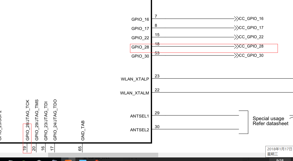
why those two PIN_18 and PIN_19 has the same name as GPIO_28?
if i want to use those pin as the I/O, how can i init ?
/*LVD_SI GPIO_23 PIN_16 JTAG_TDI
*LCD_SCL GIPO_24 PIN_17 JTAG_TDO
*LCD_RS GPIO_28 PIN_18
*LCD_CS GPIO_31 PIN_45
*LCD_RES GPIO_28 PIN_19 JTAG_TCK
*/