This thread has been locked.

If you have a related question, please click the "Ask a related question" button in the top right corner. The newly created question will be automatically linked to this question.

CC2640R2F: BLE antenna and layout guidelines

Part Number: CC2640R2F

Hello,

We are now working on a project which involves the CC2640R2FYFV MCU. We want to implement the BLE feature to exchange data with a remote laptop.

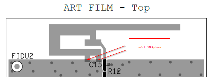
My intention was to follow the signel ended (4XS) application circuit together with its accompanying layout. Only in this case the matching network will perform optimal I guess?
The components I proposed to use are;

  • C12,C13:  CBR02C129B5GAC
  • L12 : LQP15MN2N0W02
  • L21: LQP15MN15NG02
  • C14:  CBR02C120F3GAC

The only issue I now have is the antenna. Because the component height restriction is 500 (preferrable) 400um, the availability of chip antennas is very small.
I think I found one antenna which is thin enough. However it is not clear to me how to use this. It seems like this antenna still needs an 'antenna'(PCB trace/loop)...
Also, the datasheet used even more RF caps/inductors. Are these the same parts as the matching network, or extra?? (the datasheet of the antenna is given below).

TDK_BLE_ant.pdf

ANT016008LCD1575MA1

Could you give me support in the use and layout of this antenna together with the MCU? Or propose a different, more simple antenna that we can use for this project? The range we need is only 10cm...

Thanks in advance!

Best regards,

Sven

  • Hi,

    You can use C15 and R12 for Antenna Matching. No need to modify any other components ( L21, C12, L12, C13 and C14). Keep all of them as it is.

    You selected Multi-Band Chip Antenna from TDK. You can use Single-band Antenna (ANT016008LCS2442MA1) only. It occupies less space. Yes, you need to follow their Recommended Layout and Matching Components (MT and FT-1).

    For our recommended Chip Antenna suppliers, please refer to Table-8 on our Antenna Application Note SWRA161.

    Thanks,
    PM
  • PM,

    First of all, thanks for your fast reply!

    What components are  you referring to as C15 and R12? I am referring to the CC2640R2F datasheet page 42 figure 7-3 (as added below).

    cc2640r2f.pdf

    Below is the layout of the single band antenna.  There are no dimensions in the image, while I guess these are quite critical (as I see something that looks like a stub next to FT-1)...
    What do you think is the less risky? Using a third party chip antenna (with no dimensions), or a trace antenna like the one from application note AN043?


    I look forward to hear from you again.

    Greetings,

    Sven

    rf_ant_ant016008lcs2442ma1_summary_en.pdf


  • Hi,

    My recommendation was based on CC2650EM-4XS Design -swrc300. The following is the link (Please see design files). It is same as the Circuit in the data sheet but with Antenna matching circuit (C15 & R12)

    Yes, I agree some dimensions are missing in the Antenna data sheet. You may contact them to get the dimensions, if you want to use it.

    Yes, using the Trace Antenna is less risky, as it is a proven design.

    www.ti.com/.../cc2650em-4xs-rd


    Thanks,
    PM
  • Best,

    At first sight, I thought it would be safer to use a chip antenna because there wouldn't be any needs to design our own antenna.
    Now, I agree that it is safer to use the reference design together with the Inverted-F antenna (DN007).

    So I think you already resolved my question. However, I still have the following :);

    1) In what case are C15 and R12 needed? Is this only to optimize the range?
    1) The circuit will finally be implemented on Silicon (component routing with RDL). Will we experience issues in this case? regarding different material properties?

    Thanks in advance!,

    Sven
  • Hi,

    1.The Antenna impedance changes from one design to other design because of PCB Layout variations, Ground Plane, surrounding components and Casing.

    C15 and R12 can be used to match the Antenna to 50 Ohms ( to correct any mismatch).

    2. When you use different materials, different Routing and different Gnd planes, it will change the Antenna impedance. In this case, you need to be very careful in matching the Antenna.

    Thanks,

    PM

  • PM,

    I have a question about the reference design.

    See the image below. These two 'rectangles' at the end points of the arrows, are these via's connected to the ground plane? They seem to be, but I don't see any dimensions on how much they should overlap the plane etc. This is also not given in the inverted F antenna application note (and I have no tooling to open the correct reference design PCB files).

    Thank you in advance,

    Sven

  • Hi,

    Yes, you can use Gnd Vias to connect it to the Ground Plane.

    You can use the Overlap size to the size of Via diameter ( 20 Mils or 40 Mils - not critical).

    Thanks,
    PM