Hi
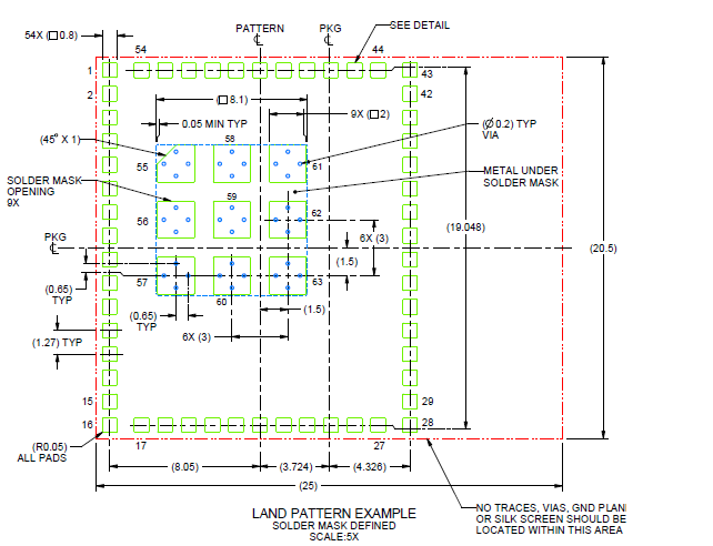
I'm currently layout on my board for the CC3220MODA module. The recommend layout specifies 4 via's in each thermal pad on the base of the module. Each via being 0.2mm (Typ). (see image below)
I guess this pad is there to wick up excess solder, so the module will sit down flat on the pcb. Now this via must be kept clear of solder resist , so the solder can wick down.
My pcb suppliers are unable to guarrantee a via with a hole size of 0.2mm will remain clear after the solder resist process. In fact they are asking me to open up the via holes to 0.45mm, which they can guarrantee.
Now, I know I can pay a lot more money, and change the processes on pcb manufacturer to obtain this. But we are using these modules on low cost products, and we need to back to get low cost PCB manufactuer.
We like to try and stick to TI recommend pad and holes sizes, because our products are built and tested by sub contractors. If there are issues they always go back to Manufactures recommendations.
Please comment
Regards
Nick