Hi,
Our team is developing a PCB based on the CC3220MODASF12MONR module, but we found a problem in the footprint design present in the datasheet.
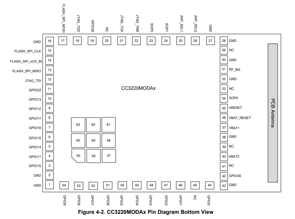
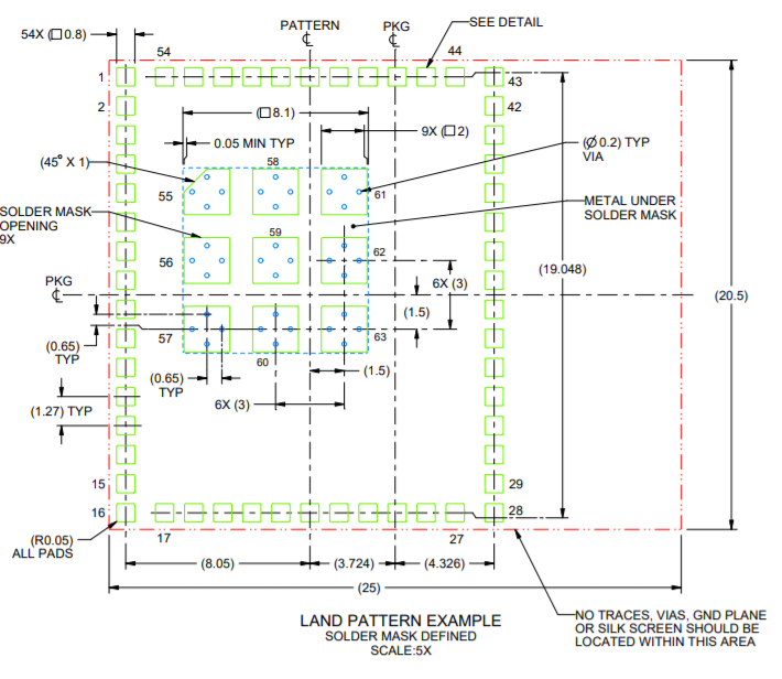
There is some incompatibility beetween the pin diagram (Figure 4-1) and the example board layout or the example stencil design. It seems that one of the images presents the bottom view and another the top view, but we could not identify which one.
We could not identify which one represents the top view of the module to desing its footprint.
Could you please identify which one represents the top view of the CC3220MODASF12MONR?
Pin diagram:
Example board layout:
Thank you for your attention,
Kremer


