Other Parts Discussed in Thread: UNIFLASH, CC3220S, CC3200, CC3220MOD
I am using the CC3220SF microcontroller (secure with chip internal/XIP flash) on a custom board.
On about two out of ten of these boards, the chip internal flash is not working/not available: The flash can not be erased using the UniFlash tool and the debugger scripts of the Code Composer Studio (CCS) report a timeout while flashing (mostly on address 0x0100000, the flash header).
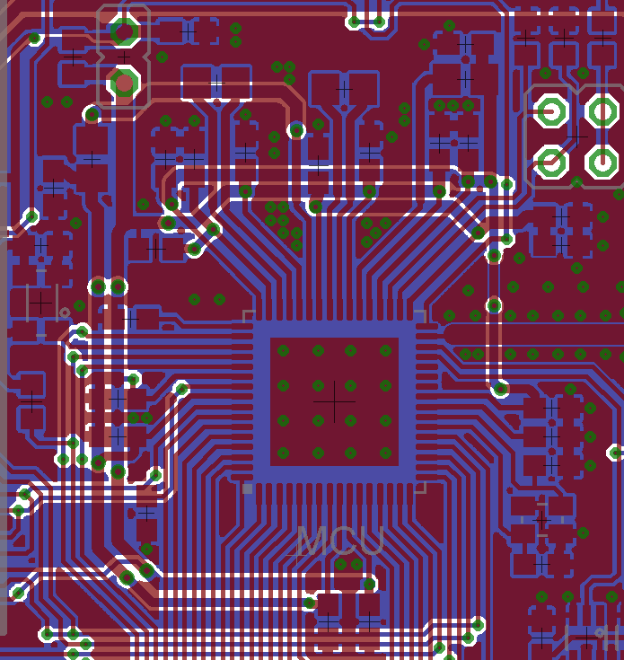
Here is a picture of the layout of my custom board:
I spent already many hours of finding the issue, but without any success.
What I found out alredy:
1. Replacing the CC3220SF on the faulty boards does not help.
Either the issue is on the board. Or all my remaining CC3220SF have the same issue with the internal flash.
2. Replacing the external SPI flash on the faulty board does not help.
3. The faulty boards/faulty CC3220SF MCUs work as expected if using the external SPI flash for the user program.
For this I changed the linker script to cc3220s.cmd and the according target configuration for the CC3220S.
4. On some faulty boards, the DC/DC converter for the flash voltage just make some switches and the gives up.
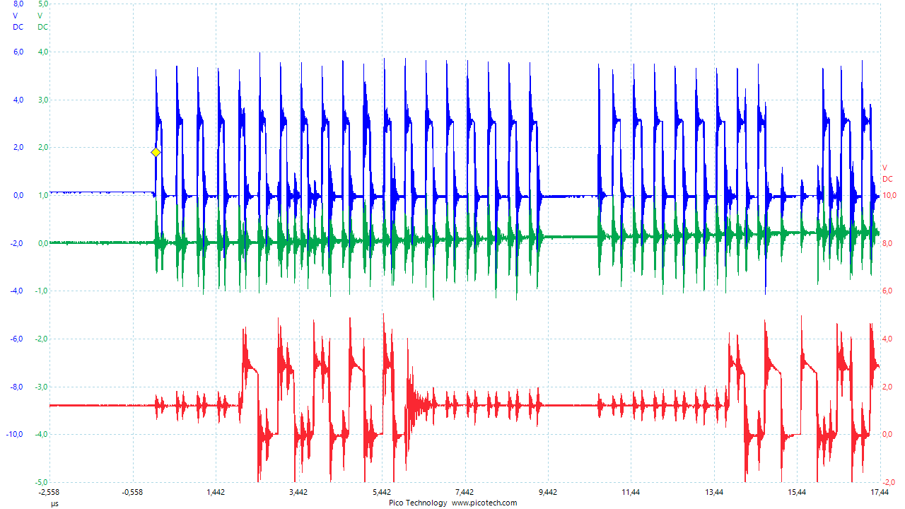
The picture below shows the voltages on some pins of such a faulty board:
Channels: channel 1 (blue): DCDC_ANA2_SW_P (pin 45), channel 2 (red): DCDC_DIG_SW (pin 43), channel 3 (green): VDD_ANA2 (green).
The spikes on all channels are due to crosstalks on the measuring wires.
The picture shows that the DC/DC converter for the flash voltage (channel 1, blue) makes some switches and the flash voltage increases a bit (channel 3, green). But than the DC/DC converter stops and the flash voltage remains constant (i.e. there can not be a short on this voltage).
On some other faulty boards/MCUs, the DC/DC converter for the flash voltage does not make any switches, i.e. the flash voltage is 0.
The picture below shows the voltages on the same pins on a working board where the chip internal flash is available (can be erased and programmed).
5. On the faulty boards using the external SPI flash for the user program (see point 3 above), I tried to erase and program the internal flash in the user program using functions of the DriverLib, but without any succuess: the function FlashErase stays in its while loop.
My questions now:
A. Is this issue "chip internal flash not available" already known? Are there any work arounds?
B. Can you give me hints to read out some registers of the flash controller or global registers (e.g. GPRCM or HIB*) to find more details of the status of the DC/DC converter for flash and the flash controller?
Like the registers GPRCM_BASE + GPRCM_O_TOP_DIE_ENABLE, HIB1P2_BASE + x in the FlashDisable function, which are not documented in the reference manual.
C. Should I inspect the voltage on other special pins?
I already inspected the voltage on a lot of pins (e.g. , but with no luck.