This thread has been locked.

If you have a related question, please click the "Ask a related question" button in the top right corner. The newly created question will be automatically linked to this question.

CC3220S: CC3220S ADC

Part Number: CC3220S

Hi TI

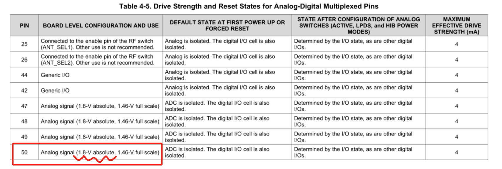
  There are one questions about CC3220S ADC that need help to answer. According to the official data of TI, the maximum allowable analog voltage of CC3220S ADC cannot exceed 1.8v, otherwise it will be damaged. However, I did the pressure test, input 2.1v with the stabilized power supply, and then conducted ADC sampling every second, which was performed for many times. However, it was not damaged. I want to know the reason. why is this I/O not corrupted?Awaiting for your reply Thank you very much!

  • felix,

    Exactly which pins have you used for this experiment?

    When you say that is it not damaged, are you still getting consistent accurate readings?

    Have you tested the ADC's accuracy with inputs 0 to 1.46V before and after you applied 2.1V to compare the difference? As the documentation states, an input higher than 1.4V can cause clipping/distortion. 

    The datasheet may state that the CC3220 can tolerate up to 1.8V to ensure customers do not use anything too much higher, but perhaps it is actually tolerant up to another 0.3V. I would not try going any higher than that to prevent accidental damage to the ADC inputs.

    BR,

    Seong

  • Hi Seong

    Thanks for your reply.

    1, I test pin50  GPIO5/ADC_CH3.

    2, Yes, I'm sure there's no damage. When I turn down the voltage (less than 1.4v), I get the correct value of ADC.

    3, I do this test because the factory production process, some CC3220S damaged (pin50), defective rate reached 5%. This pin is configured as analog input sampling ambient light (light activated triode is highest in bright light output voltage of 1.8 V). So far we don't know why this pin will be damaged. Can you give me some advice?What else is possible from an engineering point of view?

    Felix

  • felix,

    To be clear, are you troubleshooting a CC3220S? Or CC3220MODS?

    The CC3220S's GPIO5 pin is pin 60. The CC3220MODS's GPIO5 pin is pin 50.

    BR,

    Seong

  • Hi Seong

    Sorry, I didn't speak clearly. Correct that we use   CC3220S and the damaged is pin60, not pin 50.

  • felix,

    How is the ADC_CH3 pin connected to the triode? Can you share the schematic?

    What is the light sensor's part number? 

    I'd like to better understand the circuitry before making any assumptions. Please provide as much information as possible.

    BR,

    Seong

  • Hi Seong

    I would like share the schematic and the waveform:

    In the schematic, AMB_Sens connect to the CC3220S pin 60.  In daytime mode, the output voltage of the AMB Sens is about 1.8V.  The first wave shows the normal wave. The second waveform shows the AMB_Sens waveform when it is subject to power fluctuations.

    I have two question:

    1, pin60 is Hi-Z after the CC32220S power on initialization. In this state, the limiting voltage of pin60 is 3.6V, Is that right?

    2, In my firmware, When I need to configure PIN60 as ADC and convert its input voltage to analog-to-digital, I execute the following library functions:

    ADC_Handle ADC_open(uint_least8_t index, ADC_Params *params);

    After I get the voltage value of photosensitive transistor,I execute the following library functions:

    extern void ADC_close(ADC_Handle handle);

    So after that what state is pin60?Isn't it in Hi-Z?

  • felix,

    I understand that you've tried a stress test by applying a voltage up to 2.1V to the ADC and found that the device is working fine. You've also designed your system so that your ADC signal can be as high as 1.8V. However, according to our documentation, the recommended ADC input voltage is 0~1.5V and not up to the absolute max voltage of 1.8V. It is good EE practice to always follow a manufacturer's guidelines and the recommended operating conditions, and not the absolute max ratings.

    As you'll be able to see from our CC3220 reference design, we have a Voltage Follower OpAmp at each ADC input. At the input of the Voltage Follower is the Voltage Divider that will step down the analog signal. See below.

    A Voltage Follower is highly recommended for ADC input protection and when you're using a Voltage Divider. Without a Voltage Follower, your 1k||100k Voltage Divider here will not work properly either. This page explains this and why you may be seeing a max voltage of 1.84V at AMB_Sense. Your scope shot also shows that the voltage at the AMB output can swing as low as -1.24V, which can also damage the device.

    If your NPN also has high switching speed, it will have a high di/dt ramp which could cause voltage surges with parasitic inductance.

    With that said, I believe your failure rate can be significantly decreased by improving your ADC input circuit to avoid all possible risks.

    Another side note on voltage followers, the ADC pins will draw a current spike from the external source while sampling and this can cause errors in measurement. The voltage follower + RF circuit in front of the ADC is used as the ADC pins require external signal conditioning. Refer to the  standard SAR ADC app note for more information.

    BR,

    Seong

  • Hi Seong

    Thanks so much for your advice!  We consider modifying the circuit and PCB.  

     please answer these two questions:

    1, pin60 is Hi-Z after the CC32220S power on initialization. In this state, the limiting voltage of pin60 is 3.6V, Is that right?

             2, In my firmware, When I need to configure PIN60 as ADC and convert its input voltage to analog-to-digital, I execute the following library functions:

                 ADC_Handle ADC_open(uint_least8_t index, ADC_Params *params);

                 After I get the voltage value of photosensitive transistor,I execute the following library functions:

                 extern void ADC_close(ADC_Handle handle);

                So after that what state is pin60?Isn't it in Hi-Z?

  • felix,

    The digital IOs on pins 57 through 60 are always connected and must be made Hi-Z before enabling the ADC switches, so yes, the max high-level input voltage is Vdd+0.5V. 

    Yes, calling ADC_close() handles the pinmuxing of the pin back to an unassigned Hi-Z state.

    More information about TI drivers can be accessed in the SDK at /docs/tidrivers/tidriversAPIs.html

    BR,

    Seong