Other Parts Discussed in Thread: UNIFLASH, TMDSEMU110-U, CC3220SF-LAUNCHXL, CC3220SF
Hi Texas Instruments.
I am designing a board for the CC3220MODASF module.
I added the FTSH-105-01-F-D-K connector to the board design for the JTAG function.
I found some posts on the forum that says that the module's serial FLASH can only be programmed through the SPI-FLASH or UART interface.
I have a few questions about the serial FLASH programming process:
1 - Is there no way to program the serial FLASH by JTAG?
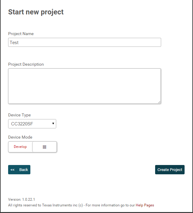
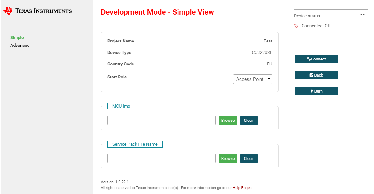
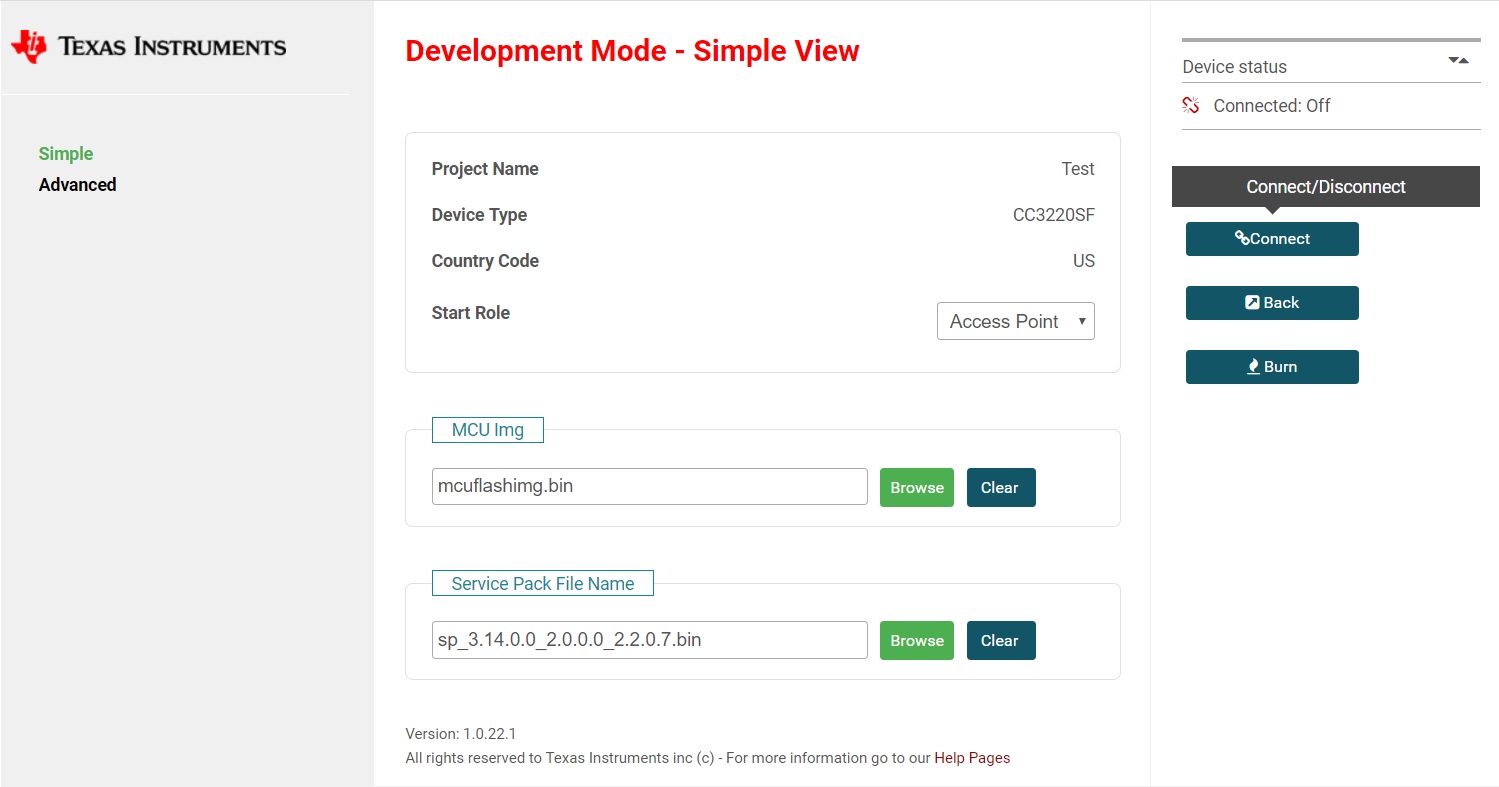
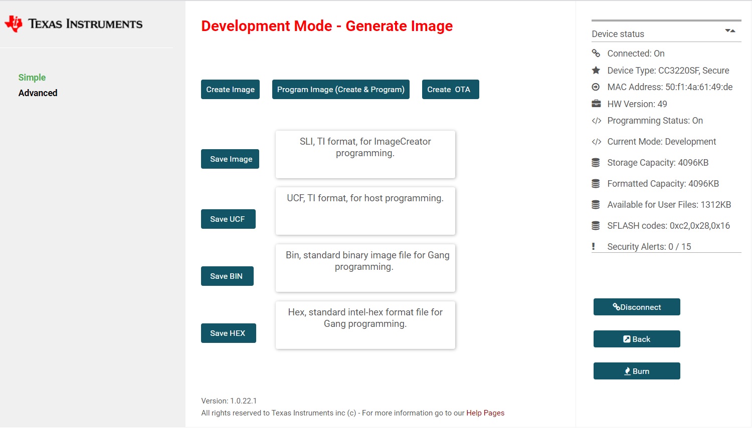
2 - I also read that the recording image can be of two types: development or production. What is the difference between these versions? Once I record a production type image, the CC3220 module's JTAG interface is permanently disabled or I can go back recording a development image on top to have the JTAG function again?
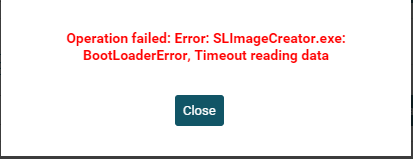
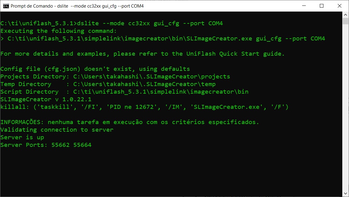
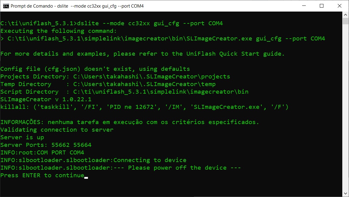
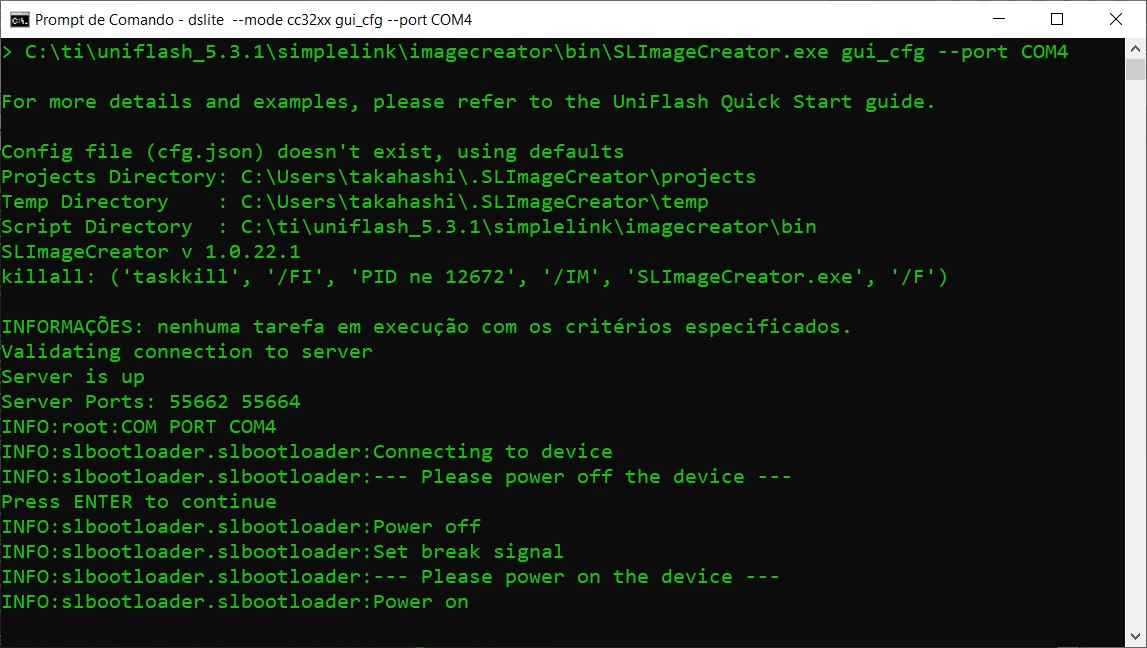
3 - I purchased the XDS110-JTAG Probe, it has a 14-pin auxiliary interface with UART interface. Can I use it to program the serial FLASH memory through this UART interface?
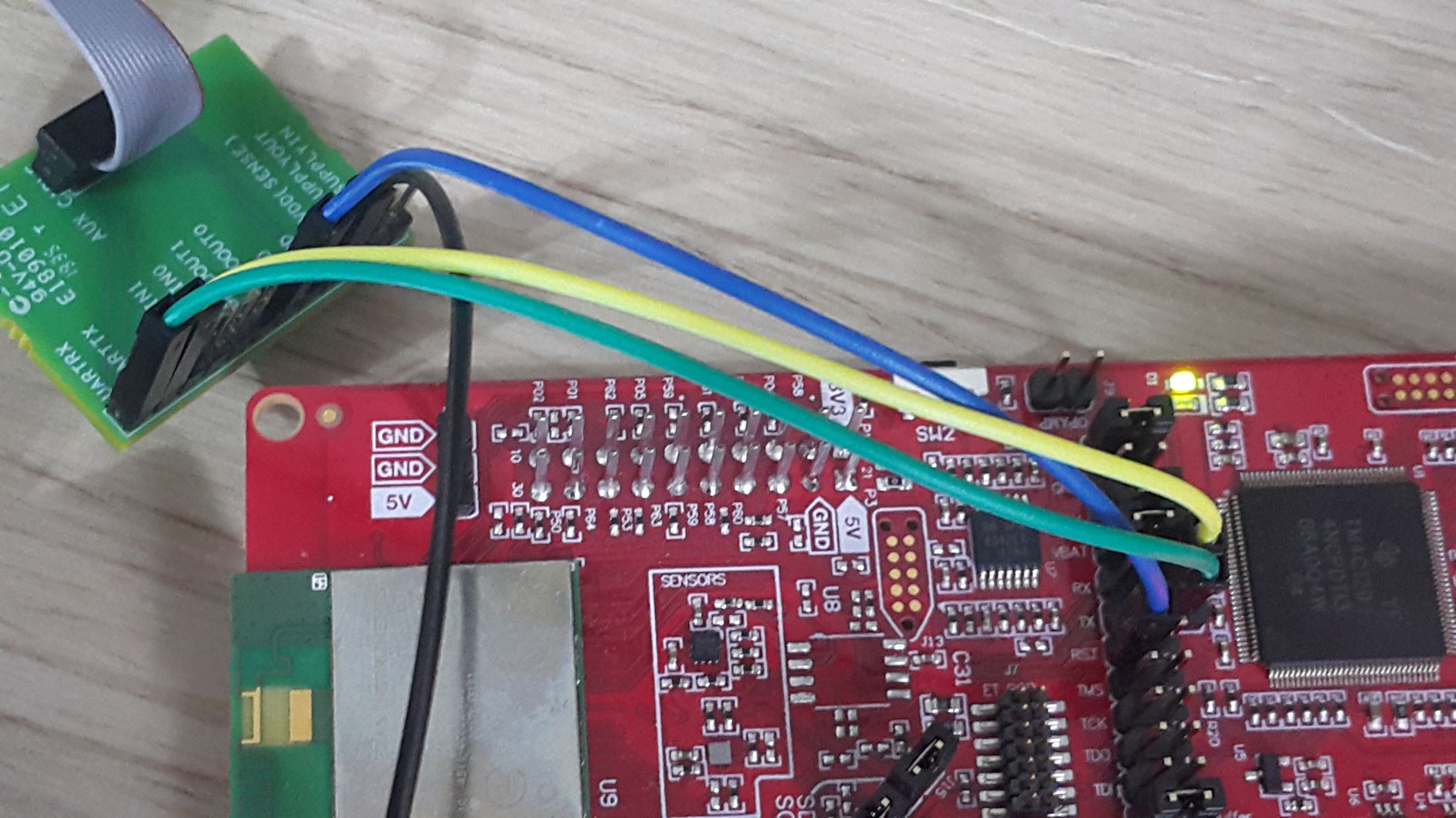
4 - If the answer to the previous question is yes, I drew a diagram to provides power, reset and image transfer using the AUX BREAKOUT card that comes with the Probe, can you check the connections?
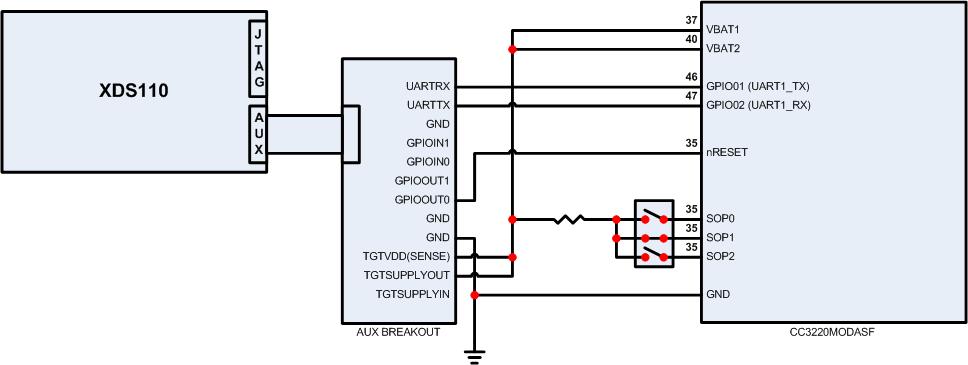
4.1 - I connected TGTSUPPLYOUT to power supply my board. I connected TGTVDD(SENSE) together because I saw this tip in another post and it also worked for me;
4.2 - I am configuring the SOPs pins using DIP switches / jumpers. Can I use the GPIOOUT1 output to momentarily control SOP1 during the serial FLASH recording process?
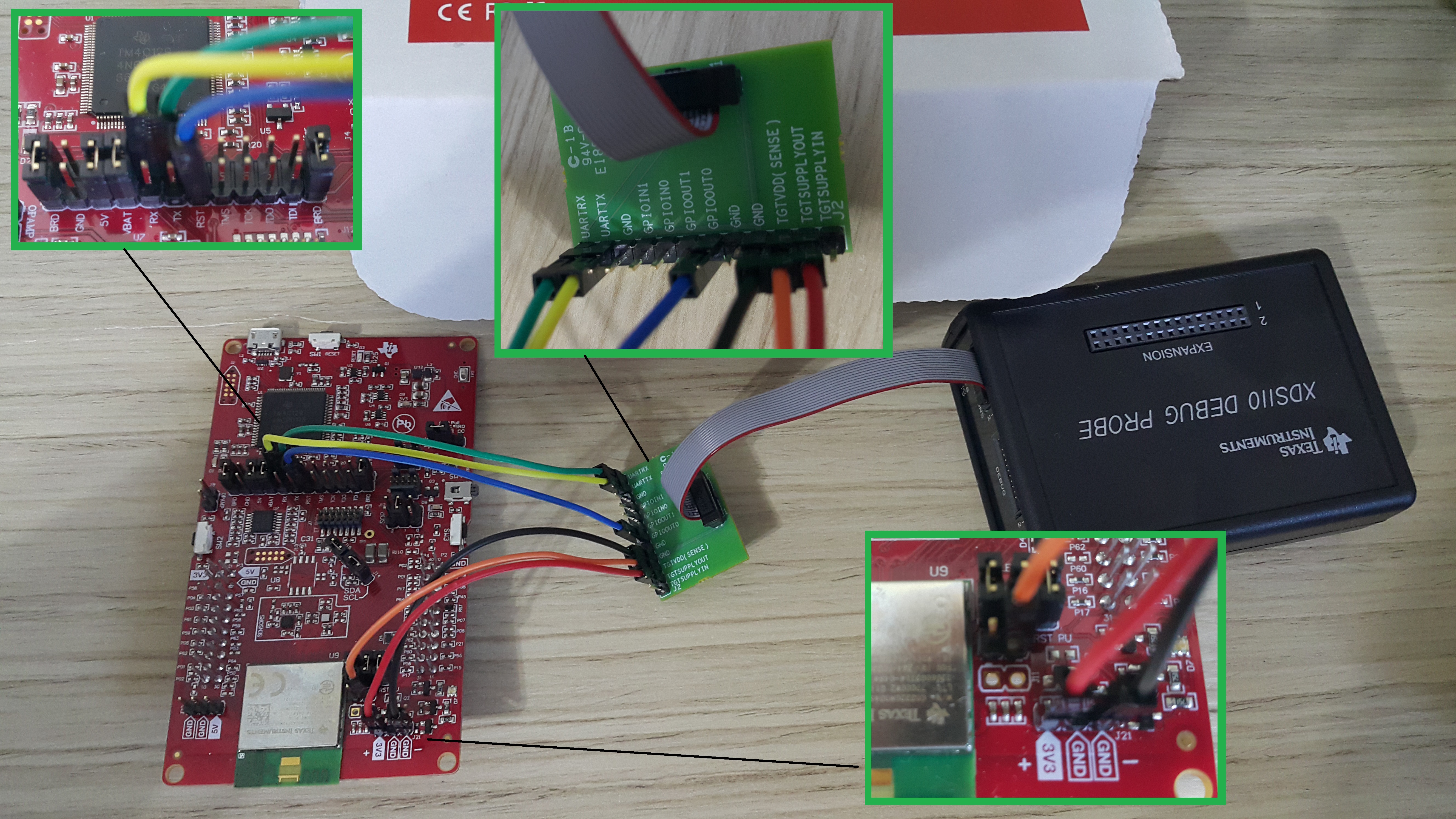
I made the connections with a CC3220MODASF LaunchPad to illustrate.
Description of cable colors:
Black: GND;
Red: TGTSUPPLYOUT -> VBATs;
Orange: TGTVDD(SENSE) -> VBATs;
Blue: GPIOOUT0 -> nRESET;
Yellow: UARTTX -> GPIO02;
Green: UARTRX -> GPIO01.
5 - If I can use GPIOOUT0 to generate nRESET. Can I also use the UniFlash software to automatically control this pin? If so, how I do it?
Thank you.