This thread has been locked.

If you have a related question, please click the "Ask a related question" button in the top right corner. The newly created question will be automatically linked to this question.

CCS/CC3220SF: UniFlah I get the following error "Operation failed: Error: SLImageCreator.exe: BootLoaderError, Timeout reading data"

Part Number: CC3220SF
Other Parts Discussed in Thread: UNIFLASH

Tool/software: Code Composer Studio

I build 4 custom prototypes with the IC CC3220SF with the Pregegulated 1.85-V Mode setting shown on page # 72 of the CC3220 datasheet

of which only one of the prototypes can I connect with the UniFlash_sl.5.3.1.2665 software and I can program it

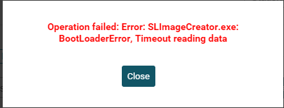
when I try to connect to the other 3 prototypes in UniFlah I get the following error
"Operation failed: Error: SLImageCreator.exe: BootLoaderError, Timeout reading data"

Could you tell me how I can solve the problem,
do you have any guide or checklist of what I have to review please

  • Hi,

    We will look into it and get back to you ASAP. Please bear with us.

    Thanks,

    PM

  • Hi Alvaro,

    Here are links to our design checklist and layout guidelines:

    http://www.ti.com/lit/zip/swru462 

    https://www.ti.com/lit/ug/swru458/swru458.pdf?ts=1588176277466 

    The 1.85V preregulated voltage mode is a mode of operation of the device in which the on-chip regulators are bypassed. There are stricter requirements for powering the device in this mode so there is not necessarily a range, and it is important to pay attention to the notes in the datasheet:

    • Load current capacity ≥900 mA 
    • Line and load regulation with <2% ripple with 500-mA step current and settling time of < 4 µs with the load step 

    note that your voltage should be more like 1.89V if you choose to use this mode. The quoted 1.85V is the minimum operating voltage, so when accounting for +/- 40mV of ripple your nominal voltage should be 1.89V 

    Thanks,
    Alexis

  • I am using the guide "CC3220 Production Line Guide" (http://www.ti.com/lit/an/swra568/swra568.pdf

    to program my prototypes following the connections on page 4 section 5.4 "UART Hardware Connection Using the CC3220 LaunchPad"

    If the Pregegulated 1.85-V Mode needs 1.89v of nominal voltage, and the CC3220SF LaunchPad has 3.3v power at the voltage terminals, how do I feed my prototypes during programming using CC3220SF LaunchPad?

    How do I connect my prototypes to the launchpad is:

    Doesn't it require 3.3v and GND for programming between the launchpad and my prototype?

  • Hi

    In the "design checklist" (www.ti.com/.../swru462) I found the following differences:
    1: The "Frequency 40MHz, ESR <60 Ohms, Load cap <12pF" that is connected to pins # 22 and 23, is different from the one I am using, the one I am using is the model: "FH4000074Z" (datasheet: https : //www.diodes.com/assets/Datasheets/FH.pdf)

    2: I have the GPIO pins on the air without connecting them in your "design checklist" it says:
    (Add 2.7K or stronger pull-up or pull-down to ensure that the state of the line is maintained during power on reset. Without a pull-up / pull-down, the line can get pulled by internal pulls momentarily casuing a glitch which lasts upto 15ms)

    3: I do not have pins 16,17,20 connected
    -I have pin # 19 connected to a pull down resistor "Res, 2.7 k, 5%, 0.063 W, 0402" model: CRCW0402270RJNED
    in his "design checklist" he says:
    Header or TP should be provided for device pins 16, 17, 19 and 20. Device also support 2 wire SWD and can be used if your design is short on GPIOs
    Function Dev Pin GPIO #
    JTAG_TDI 16 GPIO23
    JTAG_TDO 17 GPIO24
    JTAG_TCK 19 GPIO28
    JTAG_TMS 20 GPIO29

    4: PINS 40, 41 and 42 ARE NOT CONNECTED SO IT APPEARS ON THE SCHEMATIC OF PAGE 72 OF THE CC3200SF DATASHEET IN "ypical Application Schematic — CC3220x Preregulated, 1.85-V Mode"

    5: the (De-coupling capacitor = 4.7uF, 6.3V) THAT SPECIFIES, RECOMMENDING MODEL CL05A475MQ5NRNC
    IN THE MEDI MEASUREMENT
    c3 = 5.3uf
    c4 = 5.2uf
    c5 = 5.2uf
    NOTE: THE MODEL WE USE IS: (CL05A475KP5NRNC)

    6:The crystal model that is connected to pins 51.52 "Frequency 32.768KHz, ESR <150K Ohm, load capacitance <20pF" that I am using is: "ABS07-32.768KHZ-9-T"

    I have looked for the crystal that you recommend and it has a different Load Capacitance, the one that you would recomend has 12pF vs ours has 9pF


    QUESTIONS:
    Q1: The crystal that I am using can be the root cause of the problem that I have?

    Q2: The problem can be caused by the GPIO pins being on the air?

    Q3: Can pins 16,17,20 be the root cause of the problem I have?

    Q4: Pins 40, 41 and 42 as specified by the datasheet, could it not be the root cause of the problem ???

    Q5: The capacitors c3, c4, c5 that are connected to pins 37,39,44 of the MCU could be the root cause of the problem?
    -How much tolerance must these capacitors have?

    Q6: The model of the crystal that is connected to pins 51.52 that I am using is: "ABS07-32.768KHZ-9-T"

    Could it be the root cause of the problem?

  • Hi

    In the "design checklist" (www.ti.com/.../swru462) I found the following differences:
    1: The "Frequency 40MHz, ESR <60 Ohms, Load cap <12pF" that is connected to pins # 22 and 23, is different from the one I am using, the one I am using is the model: "FH4000074Z" (datasheet: https : //www.diodes.com/assets/Datasheets/FH.pdf)

    2: I have the GPIO pins on the air without connecting them in your "design checklist" it says:
    (Add 2.7K or stronger pull-up or pull-down to ensure that the state of the line is maintained during power on reset. Without a pull-up / pull-down, the line can get pulled by internal pulls momentarily casuing a glitch which lasts upto 15ms)

    3: I do not have pins 16,17,20 connected
    -I have pin # 19 connected to a pull down resistor "Res, 2.7 k, 5%, 0.063 W, 0402" model: CRCW0402270RJNED
    in his "design checklist" he says:
    Header or TP should be provided for device pins 16, 17, 19 and 20. Device also support 2 wire SWD and can be used if your design is short on GPIOs
    Function Dev Pin GPIO #
    JTAG_TDI 16 GPIO23
    JTAG_TDO 17 GPIO24
    JTAG_TCK 19 GPIO28
    JTAG_TMS 20 GPIO29

    4: PINS 40, 41 and 42 ARE NOT CONNECTED SO IT APPEARS ON THE SCHEMATIC OF PAGE 72 OF THE CC3200SF DATASHEET IN "ypical Application Schematic — CC3220x Preregulated, 1.85-V Mode"

    5: the (De-coupling capacitor = 4.7uF, 6.3V) THAT SPECIFIES, RECOMMENDING MODEL CL05A475MQ5NRNC
    IN THE MEDI MEASUREMENT
    c3 = 5.3uf
    c4 = 5.2uf
    c5 = 5.2uf
    NOTE: THE MODEL WE USE IS: (CL05A475KP5NRNC)

    6:The crystal model that is connected to pins 51.52 "Frequency 32.768KHz, ESR <150K Ohm, load capacitance <20pF" that I am using is: "ABS07-32.768KHZ-9-T"

    I have looked for the crystal that you recommend and it has a different Load Capacitance, the one that you would recomend has 12pF vs ours has 9pF


    QUESTIONS:
    Q1: The crystal that I am using can be the root cause of the problem that I have?

    Q2: The problem can be caused by the GPIO pins being on the air?

    Q3: Can pins 16,17,20 be the root cause of the problem I have?

    Q4: Pins 40, 41 and 42 as specified by the datasheet, could it not be the root cause of the problem ???

    Q5: The capacitors c3, c4, c5 that are connected to pins 37,39,44 of the MCU could be the root cause of the problem?
    -How much tolerance must these capacitors have?

    Q6: The model of the crystal that is connected to pins 51.52 that I am using is: "ABS07-32.768KHZ-9-T"

    Could it be the root cause of the problem?