Hi, I'm trying to create my custom PCB using the CC3200R1M1RGCR and the XDS100v3 debugger.
I've posted my schematic here.
I placed PFET for reverse battery protection. I use a 9V battery.
I use a buck converter, a motor driver, and a 6-axis accelerometer via I2C.
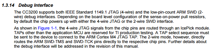
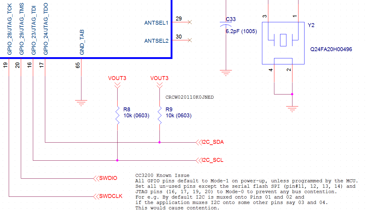
I have to use many GPIOs so using the JTAG pins as I2C pins are inevitable. I have to use SWD with XDS100v3.
I have some questions about it.
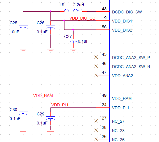
0) At pin 45 (DCDC_ANA2_SW_P), the CC3200 launchpad does not populate an inductor.
I'm not planning to use the pin 45 as GPIO_31. Should I place an inductor?
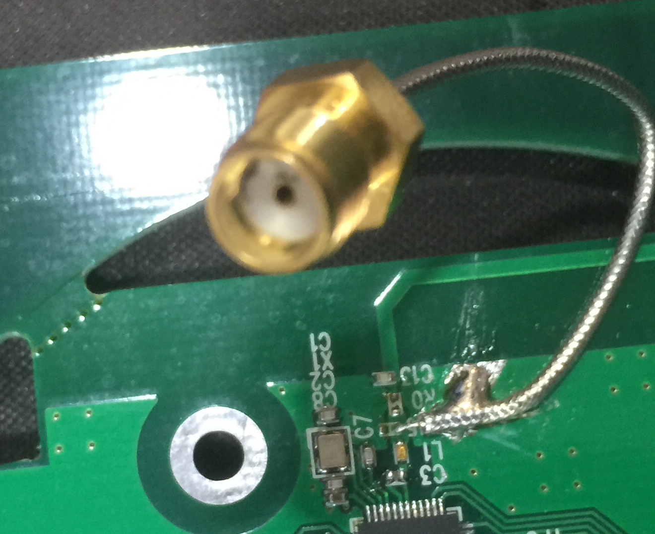
1) I removed all the SMA connectors in my schematic. Should I populate one?
2) I noticed that the ADC channels' max input is 1.5V. I placed NFET and PFET for battery level checking by referencing a circuit.
Will that configuration work?
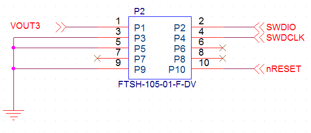
3) Also, is my TI 14 pin JTAG connection is correct?
-Best Regards