This thread has been locked.

If you have a related question, please click the "Ask a related question" button in the top right corner. The newly created question will be automatically linked to this question.

WL1807MOD: / TXS0108

Part Number: WL1807MOD


Hello community,

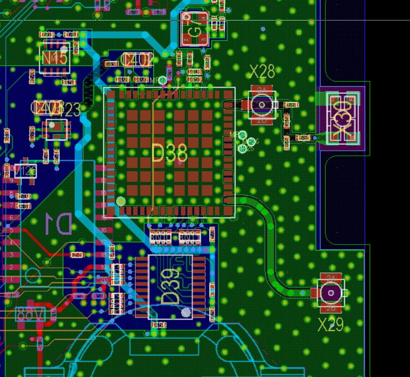
I have some trouble with our WL1807 design (see schematic attached).

When we are testing our design with higher temperature like 60 °C we get an error at initializing.

The error do not occurs at lower temperature, we also tested it in climate cabinet with 0 °C and 40 °C. The error occurs only at 40 °C above.

Our logfiles looks like:

[2019-04-19 23:41:23.928] [ 1.937343] mmc1: queuing unknown CIS tuple 0x91 (3 bytes)
[2019-04-19 23:41:23.928] [ 1.938922] mmc1: new high speed SDIO card at address 0001

[2019-04-19 23:41:28.502] [ 6.657544] fw_get_filesystem_firmware: path = /lib/firmware/updates/4.1.15-rel_imx_4.1.15_2.0.0_ga-20170202-IF40-/ti-connectivity/wl1271-nvs.bin
[2019-04-19 23:41:28.555] [ 6.693241] fw_get_filesystem_firmware: file = 0xfffffffe, IS_ERR = 1
[2019-04-19 23:41:28.555] [ 6.699699] trying next...
[2019-04-19 23:41:28.751] [ 6.715314] fw_get_filesystem_firmware: path = /lib/firmware/updates/ti-connectivity/wl1271-nvs.bin
[2019-04-19 23:41:28.751] [ 6.732582] fw_get_filesystem_firmware: file = 0xfffffffe, IS_ERR = 1
[2019-04-19 23:41:28.751] [ 6.743539] trying next...
[2019-04-19 23:41:28.751] [ 6.752620] fw_get_filesystem_firmware: path = /lib/firmware/4.1.15-rel_imx_4.1.15_2.0.0_ga-20170202-IF40-/ti-connectivity/wl1271-nvs.bin
[2019-04-19 23:41:28.751] [ 6.766529] fw_get_filesystem_firmware: file = 0xfffffffe, IS_ERR = 1
[2019-04-19 23:41:28.751] [ 6.774324] trying next...
[2019-04-19 23:41:28.751] [ 6.777504] fw_get_filesystem_firmware: path = /lib/firmware/ti-connectivity/wl1271-nvs.bin
[2019-04-19 23:41:28.751] [ 6.787386] fw_get_filesystem_firmware: file = 0xa896d3c0, IS_ERR = 0
[2019-04-19 23:41:28.751] [ 6.795109] fw_get_filesystem_firmware: path = /lib/firmware/updates/4.1.15-rel_imx_4.1.15_2.0.0_ga-20170202-IF40-/ti-connectivity/wl18xx-conf.bin
[2019-04-19 23:41:28.751] [ 6.809269] fw_get_filesystem_firmware: file = 0xfffffffe, IS_ERR = 1
[2019-04-19 23:41:28.751] [ 6.815995] trying next...
[2019-04-19 23:41:28.751] [ 6.818878] fw_get_filesystem_firmware: path = /lib/firmware/updates/ti-connectivity/wl18xx-conf.bin
[2019-04-19 23:41:28.751] [ 6.828389] fw_get_filesystem_firmware: file = 0xfffffffe, IS_ERR = 1
[2019-04-19 23:41:28.753] [ 6.835086] trying next...
[2019-04-19 23:41:28.753] [ 6.838258] fw_get_filesystem_firmware: path = /lib/firmware/4.1.15-rel_imx_4.1.15_2.0.0_ga-20170202-IF40-/ti-connectivity/wl18xx-conf.bin
[2019-04-19 23:41:28.753] [ 6.852046] fw_get_filesystem_firmware: file = 0xfffffffe, IS_ERR = 1
[2019-04-19 23:41:28.753] [ 6.859054] trying next...
[2019-04-19 23:41:28.753] [ 6.862174] fw_get_filesystem_firmware: path = /lib/firmware/ti-connectivity/wl18xx-conf.bin
[2019-04-19 23:41:28.754] [ 6.871360] fw_get_filesystem_firmware: file = 0xa896db40, IS_ERR = 0
[2019-04-19 23:41:28.754] [ 6.887367] FAT-fs (mmcblk0p1): Volume was not properly unmounted. Some data may be corrupt. Please run fsck.
[2019-04-19 23:41:28.766] [ 6.919626] wlcore: ERROR couldn't get hw info

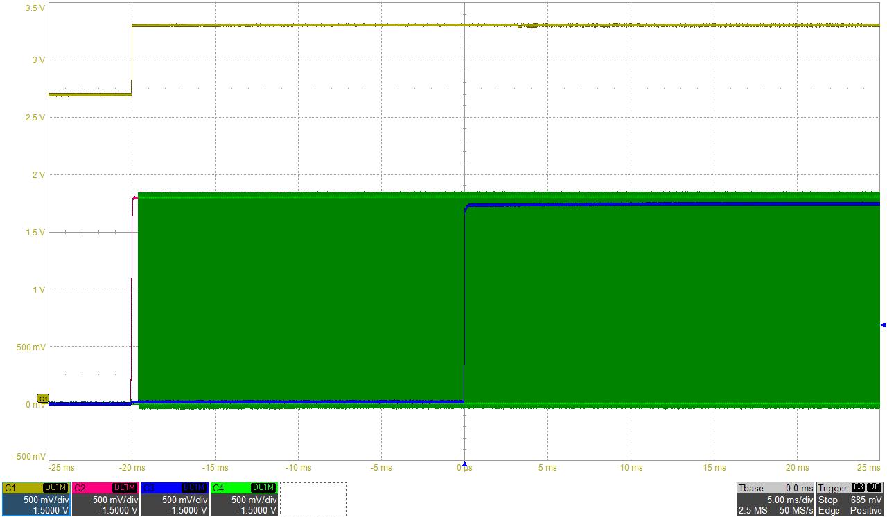
The SDIO-Interface recognize the WL1807 but it seems that the error will occuring while loading the firmware.

I also tested to add 10k pullups at CMD, CLK and DATA0-3 on 1.8V logic, 3.3V logic and as well on both sides at the same time.

But the error still occurs.

I need some help.

Thank you in advance.

Best regards,

Juergen 

WL1807_Schematic.pdf

  • Hey Juergen,

    Have you tried probing your voltage rails with an oscilloscope during this operation? Your circuit at pins 38, 46, and 47 is elaborate compared to our reference design which should be followed as closely as possible.

    In addition, have you followed our recommended guidelines outlined in Table 7-2 in the datasheet? 

    BR,

    Seong

  • Juergen,

    In addition, I'd like to understand your set up. How are you connecting the SD2_xx traces? FYI - ribbon cables do not work well and you must ensure that the cables you are using are not too long and rated for high temp.

    BR,
    Seong
  • Hello Seong,

    at first thanks for your reply.

    The design include a module with board-to-board connector, and the SD2-Interface is working well with a starterkit.

    The CPU is an i.MX6D.

    Yes I have already checked the signal with a probe.

    The following figure shows:

    Yellow = V_3V3_WLAN (VBAT_IN) ; red = V_1V8_WLAN (VIO_IN) ; blue = WLAN_EN_1V8 (WLAN_EN) ; green = EXT_32k (32.768 kHz oscillator)

    I also checked the SDIO-Interface (1.8V-logic)

    yellow = SDIO_CMD_1V8 (WL_SDIO_CMD_1V8) ; red = SDIO_CLK_1V8 (WL_SDIO_CLK_1V8) ; blue = SDIO_D0_1V8 (WL_SDIO_D0_1V8)


    I also followed your guidelines:

    As i mentioned before, under 60 °C it works fine. It is just while booting under > 60 °C ambient. 

    But what I have seen is, when I add a probe on the 1.8V-logic interface (CLK / CMD) the WL1807 will also boot at > 60 °C ambient.

    Thanks in advance!

    Best regards,

    Juergen 

  • Hello,

    I have forget to attach one more figure:

    Yellow: SD2_CLK (3.3V) from CPU measured at D39 pin 18

    Is it maybe possible that we have stressed the TXS0108 to much. According Spec there is only VCCA + 0.5V / VCCB + 0.5V allowed. And we have some peaks with 3.9V

    Because now our customer is also getting those errors.

    Thanks in advance.

    Best regards,

    Juergen

  • Hi Juergen,

    1) Are the blue dots on your layout vias? Or soldermask opened testpoints?

    2) From reading the TXS0108 datasheet, external pull-ups should not be required as the device has internal smart PU/PD resistors.

    3) From your layout, I see that there is no solid ground plane under the TXS0108. Having a solid plane minimizes inductance which is desirable for high speed signals. This also serves as a good thermal conductor and can act as a heat sink to keep thermal levels minimized.

    4) The lengths of the traces from the WL1807 to the TXS0108 could have been minimized if the TXS0108 is rotated 90 degrees counter clock wise. Also the traces that connect to WL1807's pins 6 and 7 are winding. The could possibly create a large current loop and noise along the path as well as EMI.

    BR,
    Seong
  • Hi Seong,

    1) These are testpoints / measurementpoints for easier  signal integrity measurements.

    2) I agree with you.

    3) Actually I only show you the first layer. Here a new figure with all layer shown:

    Layer 2 is GND, Layer 3 is signal, Layer 4 and 5 is VCC, Layer 6 is signal, Layer 7 is GND, Layer 8 is signal

    4) Could be...

    But what I have found out, I can't saw the WL1807 as SDIO user.

    The signals are coming through the TXS0108 through, but I can not see any kind of registration on the SDIO bus.

    Is it possible that the power-supply can destroy the WL1807 ? Because we have now 6 of 15 prototypes with "damaged" WL1807 which did not shown on the SDIO bus.

    Best regards,

    Juergen

  • Juergen,

    If the TXS0108 is on the top layer, then it does not have solid GND plane on the same layer, correct?

    How are you sourcing power to the WL1807MOD and TXS0108?

    Can you confirm that your power-up sequence follows Figure 5-2 in the datasheet? See footnote #3 -> "At least 60 µs is required between two successive device enables. The device is assumed to be in shutdown state during that period, meaning all enables to the device are LOW for that minimum duration."

    BR,
    Seong
  • Hello Seong,

    TXS0108 is on top layer, and doesn't have a "solid" GND plane, that's correct.

    I am sourcing WL1807 and TXS0108 from the LDO N15 and P-MOSFET V123, but both signal path have a EN-Signal.

    The schematic is attached in my initial post.

    The Power-Up Sequencing is shown in the second post from me:

    Yellow = V_3V3_WLAN (VBAT_IN) ; red = V_1V8_WLAN (VIO_IN) ; blue = WLAN_EN_1V8 (WLAN_EN) ; green = EXT_32k (32.768 kHz oscillator)

    As I mentioned before, we are not seeing the SDIO-Bus anymore. We also exchanged the TXS0108 with a new one to exclude the TXS0108. Still no to the SDIO-Bus.

    I am thinking that the WL1807 has been damaged because of the Power-Cycling (Power Sequencing while power up / down). 

    Is the WL1807 sensitive in relation power up/down that lead to damage?

    Best regards,

    Juergen

  • Juergen,

    Yes, failure to follow the power sequencing guidelines can damage the chip. When powering down, WLAN EN should be deasserted 10us before all supplies to the device are lowered.

    Have the guidelines under Section 5.21.2 in the datasheet been followed during your tests and measurements?

    BR,

    Seong

  • Hello Seong,

    see attached power-down and power-up sequencing. (CH1 (YELLOW) = WLAN_EN_1V8 (=WLAN_EN); CH2 (RED) = V_3V3; CH3 (BLUE) = V_3V3_WLAN (VBAT_IN); CH4 (GREEN) = V_1V8_WLAN (VIO_IN) ).

    As you can see we have more than 10µs between WLAN_EN is LOW and Power-Supply goes off.  

    The following figure shows the power up, you can see that the power supply is also stable before deassert WLAN_EN.

    It looks like we are within the specifications. Therefore, I have no clue why we have 6 boards with a damaged WL1807.

    Those 6 boards won't show up any registration at the SDIO-bus. Nor after exchange the TXS0108.

    Do you have any other suggestion, idea ?

    Best regards,

    Juergen 

  • Hey Juergen,

    The oscilloscope captures show that the power-up/power-down sequencing is not the issue.

    You provided an oscilloscope shot of the clock signal where there are noticeable ringing. This ringing will be a lot worse without the oscilloscope probe's capacitance introduced to the trace, so as you have already suspected, this could be the source of the issue. That said, could you also provide o-scope captures of the clock signal from the WiLink side?

    Taking another look at your layout, in addition to the points I made before, your trace widths look thin as well. I understand you are doing a redesign. Please share your schematic and gerbers when you have completed it.

    BR,
    Seong

  • Hello Seong,

    I have already mentioned a figure with the Clock-Signal on the WiLink side.

    Here we go again:

    I also checked the SDIO-Interface (1.8V-logic)

    yellow = SDIO_CMD_1V8 (WL_SDIO_CMD_1V8) ; red = SDIO_CLK_1V8 (WL_SDIO_CLK_1V8) ; blue = SDIO_D0_1V8 (WL_SDIO_D0_1V8)

    I think there should be no issue with that signal.

    Also I don't think that our design has problems with the trace width because we only have problems during boot-cycle. If the firmware for WL18xx is loaded there are no issues during high temperature.

    I have got from our local TI-FAE the Eval-Board "BeagleBone Green Wireless", I have tested the power-cycle with high temperature and had no problems at all. Also when the external pullups (10k) on the 1.8V (WIFI) side were removed. 

    Therefore the only difference is:

    - The Eval-Board got a GPIO for OE (levelshifter)

    - The Eval-Board got a GPIO for WL_EN (without levelshifter)

    I am not sure if this will help us. 

    Is it possible that we have to ensure that the Bluetooth interface will be disabled on the WL1807, because the BT_EN has no external pulldown (resistor is not connected). Is it possible that the BT_EN can interfere with the SDIO-Interface for WLAN?

    Best regards,

    Juergen

  • Juergen,

    1) I am not able to see the images in your previous post.

    2) Possibly - if Bluetooth is not used, you must connect BT_EN to ground.

    3) The device is detected during bootup and the SDIO bus fails during fwr download. Have you tried reducing the SDIO frequency to something lower like 1MHz? You can do this by adding max-frequency=<1000000> in dts file.

    BR,
    Seong
  • Hello Seong,

    1) sorry here again:

    yellow = SDIO_CMD_1V8 (WL_SDIO_CMD_1V8) ; red = SDIO_CLK_1V8 (WL_SDIO_CLK_1V8) ; blue = SDIO_D0_1V8 (WL_SDIO_D0_1V8)

    2) With the WL1807 there is no Bluetooth IP, therefore we can't use it. The Pulldown was not connected at this moment. It would be strange if this has an influence.

    3) Actually our customer build the SW and he said that changing the frequency in dts-file won't change the bus frequency. I am not sure why.

    Now we are making a redesign.

    Best regards,

    Juergen 

  • Juergen,

    After changing the dts-file, you must use this to build the dtb file. After creating the dtb file, you must put it in the root file system's boot folder.

    See the Linux Kernel User's Guide to learn how to build the dtb.

    Hope this helps,

    Seong