Because of the Thanksgiving holiday in the U.S., TI E2E™ design support forum responses may be delayed from November 25 through December 2. Thank you for your patience.

This thread has been locked.

If you have a related question, please click the "Ask a related question" button in the top right corner. The newly created question will be automatically linked to this question.

CC2531: What would be happen when USB DP/DM are connected during CPU power down

Part Number: CC2531

Hi TI support teams,

I am now re-designing  a previous Iot product for a certain customer .

That product  is using the CC2531 radio CPU and using embedded USB port.

I am now concerning about power on/off function change regarding USB and CPU power sequence.

Under previous specification, power on is caused by USB insert and VBUS  arise,

and power off is caused by USB connector disconnection.

This is simple and same as dongle, but the product has LiPO battery backup also , so the customer is requiring that the power on/off should be controled by a soft switch not by USB connection.

But we are concerning about problem would be happen that the USB DP/DM signal is provided on the CPU port during CPU powered down under this new specification.

I'm wondering these are USB PHY input port, therefore such situation would be allowed, right?

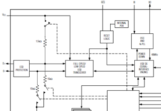
Attached pictures are USB input and CC2531 DP/DM schematic.

Could you please kindly help us ?
Your support would be highly appreciated.
Best regards,

Yoshiaki Maehara

  • Hi,

    I will look into this. 

    You can also consider using a low power PMOS to design a logic such that when the USB is plugged in the battery is out of the power loop.

    Regards,

  • Hi FI-san,

    Thank you for your respond.

    >You can also consider using a low power PMOS to design a logic such that when the USB >is plugged in the battery is out of the power loop.

    Yes, I am using PMOS to change battery power to USB power to power lane.

    Just like below link.

    https://electronics.stackexchange.com/questions/359490/p-channel-enhancement-mosfet-behaviour

    Now I am discussing about power on sequence, there is a Load switch(another pMOS) on the power lane to power the system including CPU.

    There is no problem if Load Switch would turn on when USB is connected.

    But this time we would like to change specification to power on by mechanical switch after USB is connected.

    Therefore, in this case there would occur a duration that USB Dp/DM are added to CPU pins inspite of CPU vdd = 0V.

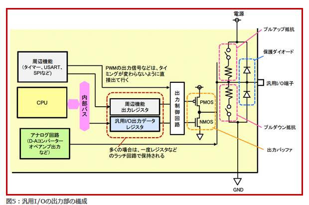
    Generaly speaking, CPU GPIOs are constructed like the picture shown below.

    (I'm sorry for Japanese drawing)

    My concern is,

    If CPU Vdd = 0V and GPIO input voltage exceed  Vdd +0.3V,  this might destroy upper protection diode.

    But I guess this is USB dedicated port, therefore port construction should be different from this general port.

    Therefore I would like you to confirm CC2531 USB PHY port specification if you could.

    Thank you very much for your support.

    And sorry for my poor English description.

    Best regards,

    Yoshiaki Maehara

  • Hi TI support team,

    Thank you for the support.

    I have tested actual Full Speed USB communication.

    Actually I don't familiar with the USB interface, but I checked using USB host IC.


    This time, I have used an MAXIM MAX3421E USB Host controller IC and

    connect to FTDI FT232RL with loop mode.


    Inside the USB host IC,it seems DP and DM are pulled down by 15kΩ.

    Therefore, if there is no peripherals, DP/DM line keeps 0V as shown below.


    When the FT232RL is connected to USB, DP is pulled up to 3.3V with 1.5kΩ pull up resister,

    this makes DP line would rise to 3.3V,

    Then USB Host detect the peripheral with DP line voltage rise and begin communication through the USB DP/DM line.

    It means until the CC2531 3.3V would be provided(also 1.5k resister), no voltage will be added to CC2531's DP/DM port.

    So I guess if USB connector is connected during CPU power is off, it is no problem

    if the 1.5kΩ DP pull up register is not activated by Vdd.

    Because DP/DM line keeps 0V in this situation.


    Is this understanding is correct?

    Your assistance is highly appreciated.

    Best regards,

    Yoshiaki