Part Number: CC2530
Other Parts Discussed in Thread: CC2538, CC2592,
I am experiencing verification errors on a design refresh (303), based on an existing functional design (302). The Erase, Erase and Write functions have worked with mixed results across various Windows installations, and SmartRF04EBs. Any read-back or verification of flash fails. We've used the latest Flash Programmer and SmartRF Studio with SmartRF04EB to communicate with the device.
The layout pays close attention to the CC2538_CC2592 EM design for relevant chip spacing and layout details.
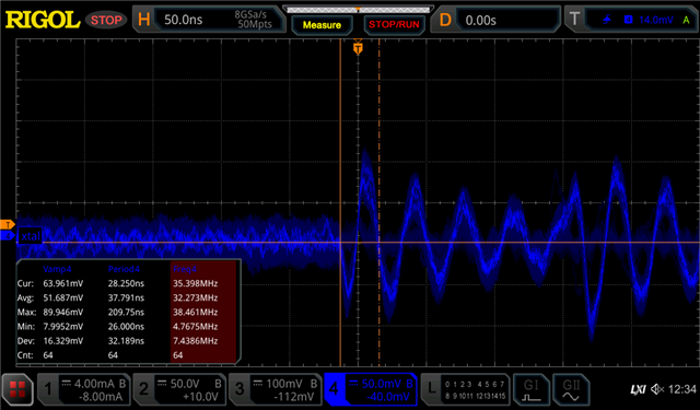
From existing TI posts on the topic, DD+DC signal integrity and 32 MHz crystal timing appear to be prevalent causes.
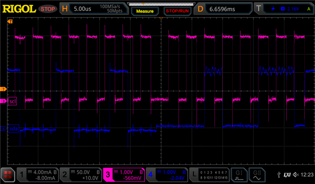
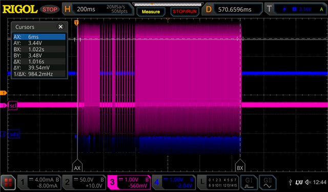
I have included oscilloscope captures of the flash write DD+DC lines, and 32 MHz crystal on the latest design and existing known-good design. I used a passive 10x, 300 MHz probe on all measurements with the DUT powered by laptop battery through SmartRF04EB.
I have layout CAD and other materials for evaluation, where useful.
302 crystal:

303 crystal:
303 DD+DC: