This thread has been locked.

If you have a related question, please click the "Ask a related question" button in the top right corner. The newly created question will be automatically linked to this question.

CC2538&CC2592 EVM LAYOUT

Other Parts Discussed in Thread: CC2538, CC2592

Hi, 

after analyzing the CC2538&CC2592 layout on pdf, I'm wondering about planes developed on signal inner layer.

  • GND plane:
    • Thermpad. There is a GND plane under QFN's thermpad.
    • Resting parts of the layer which not belong to any other signal or power line.
  • PWR plane:
    • VDD. There is defined a power plane to connect all power pins on CC2538.
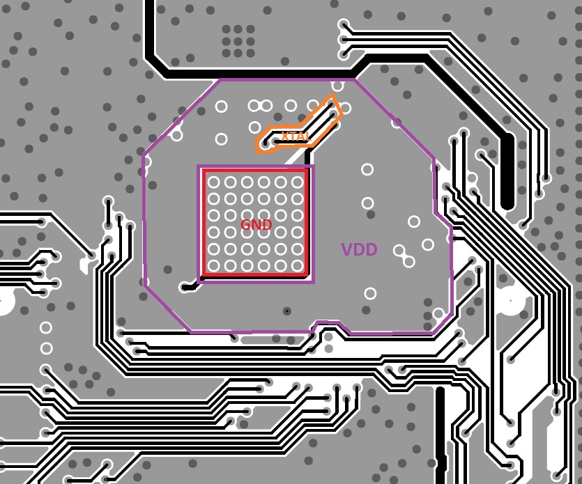
  • XTAL traces:
    • Both xtal traces for main oscillator are inside the power plane. Even when they have short length, could this 'shielding' with VDD plane affect to xtal signal integrity? Or do you assure there is no problem to do it so?

  • RF signal:
    • Power plane has some part below the RF traces, when guidelines recommend to not place nor power traces neither power planes under RF part.  does this configuration decrease the RF performance?
    • In case, CC2592 is not being used, could the power plane be placed under RF part? Or do you suggest another option?

KR!

  • Hi KR,
    XTAL traces:
    Regarding the XTAL traces, this should not pose any problem.

    RF Signal:
    In the design, the 2nd layer is a continuous ground plane which provides necessary shielding for the RF traces. The signal plane is the 3rd layer.
    Power plane should not be placed directly under the RF part.

    please also refer to the performance results of the design here www.ti.com/.../swra447.pdf

    regards,
  • Hi FI,

    thanks for your answer.

    Xtal doubt is understood.

    But about RF, even having ground plane entirely at the second layer, if there is no front end, CC2592, at design which also helps to amplify the RF signal among other features, power plane or power/signal traces below RF part could add EMI issue, and decrease its performance.

    The point is to ensure which of the two option is better for getting the highest performance in new design, taking into account the solution for C2538&CC2592 EVM, or the one for CC2538 EVM, which has routed all the power traces withouth interfering with RF part.

    What do you recommend for improving the design and later RF performance?

    Regards.

  • To be safe, it is better to have all power routing done away from the RF part but in that case big loops should also be avoided so that they don't become antennas. Having said that, the only way to verify expected EM performance is through thorough EM simulation.

    The designs on the website have been tested to extract maximum performance and we recommend that they are copied as closely as possible.

    Also, you can post the schematic and layout on the forum and we will review it for any discrepancy that may affect the performance.

  • Thanks FI.

    Then, I'm going to finish my design taking into account your suggestions.

    Regards.