This thread has been locked.

If you have a related question, please click the "Ask a related question" button in the top right corner. The newly created question will be automatically linked to this question.

CC2538: CC2538 + CC2592 2-layers Layout Review

Part Number: CC2538
Other Parts Discussed in Thread: CC2592

Hi all,

I have designed CC2538 + CC2592 module. The schematic is below:
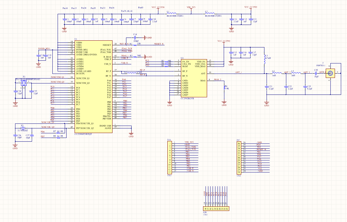
I need everyone help to review the 2-layers layout.

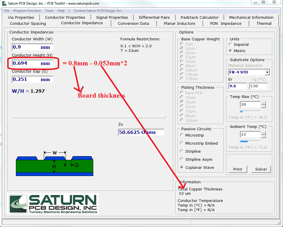
This layout is designed on FR-4 PCB, 0.8mm board thickness, 53um copper thickness. I use the Saturn PCB tool to calculate the impedance of antenna trace below:
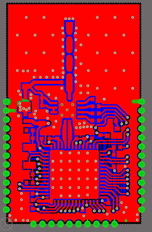
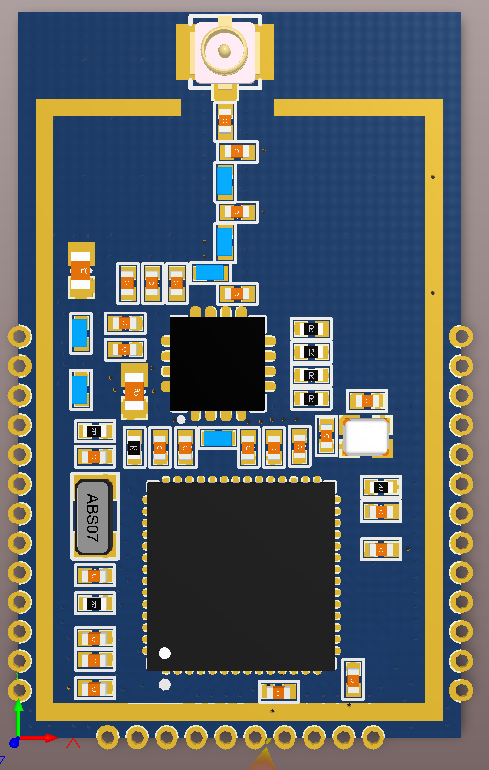
And these are the TOP, BOTTOM and 3D layer. Can everyone take the time help to review. Thank all so much.

TOP:

BOTTOM
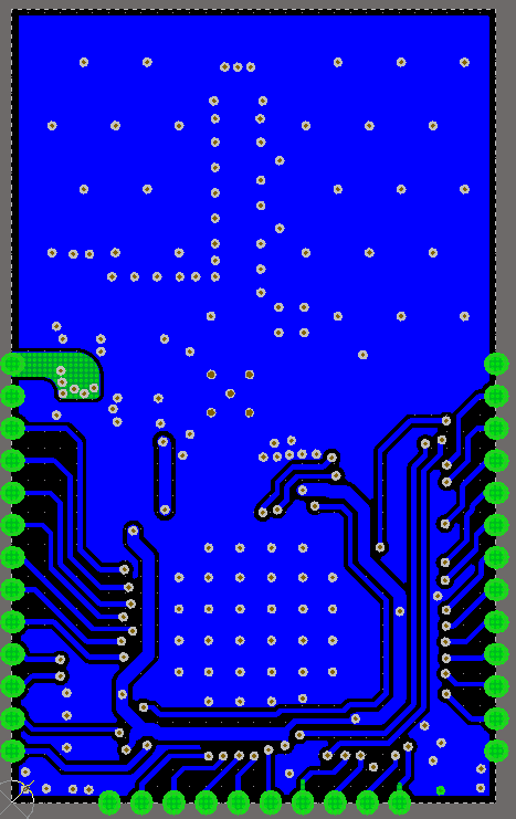
TOP + BOTTOM
3D
  • Hi,

    It looks Good except the following minor issues.

    C18 & C19 must be 1uF.

    C8 must be placed near Pin-43 ( you may move the crystal a little far to make the room for C8).

    Pins 13, 14 & 15 on CC2592 can be shorted together (Please see Ref design - SWRC286 ) and use One single trace to feed them

    Thanks,

    PM

  • Hi TI supporter,

    I have fixed these issues which is recommended by you.

    The Gerber has already sent to FAB. I will report the performance to you later.

    Thank you so much.

  • Hi  

    I am also working on CC2538+CC2592   2 layer board but by board thickness is  1.6 mm FR4,  I was  going through your blog and  is curious to  know the performance of your board . What  is the maximum  range you are getting  with the board..  In my case if it keep the board about  0.5 mtr away from the sniffer i get a  RSSI reading of -25 dBm and if I place it next to the sniffer i get a reading of -8 dBm. 

    If I keep the TI reference board next to the Sniffer I get a RSSI reading of -1 dBm, so I guess some issues with my board ..   

    Look forward for your  reply 

    Regards

    kanchan