This thread has been locked.

If you have a related question, please click the "Ask a related question" button in the top right corner. The newly created question will be automatically linked to this question.

CC2592: In-Band Emissions

Part Number: CC2592
Other Parts Discussed in Thread: CC2640,

Hi, 

I am using a CC2640/CC2592 bluetooth RF design. 

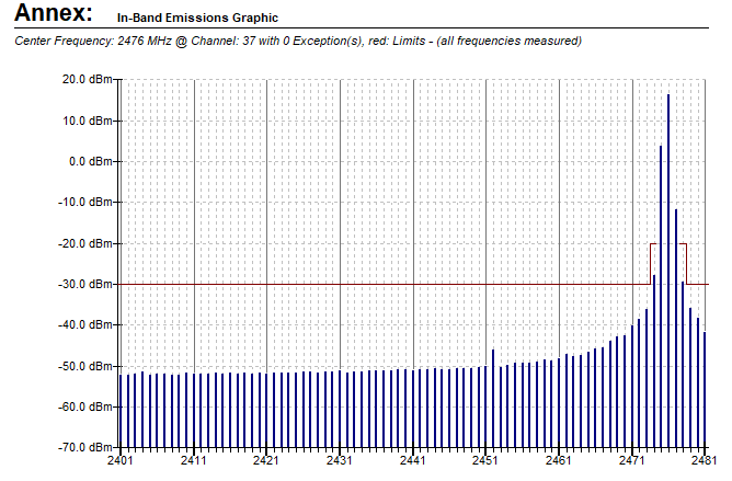
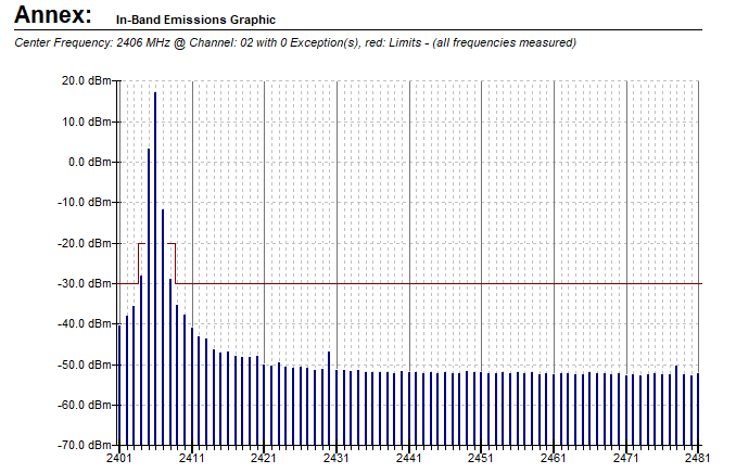
On the first board spin I had a relatively clean Rf performance, but had a few instances of unwanted in-band spurs:

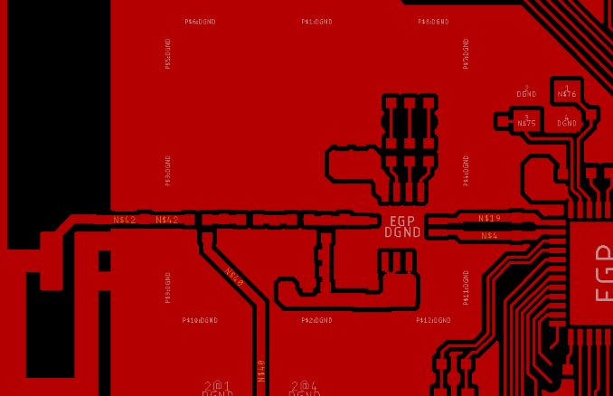
I thought this was the result of asymmetries in the layout cause by the thermal reliefs on the ground pads.
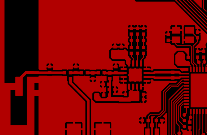
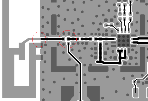
However, after removing the thermals the in-band spurs actually got significantly worse: 

The version without the thermal pads, is actually closer to the TI reference design. The reference design does not have these.

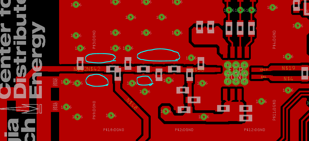
Any ideas? Do I need to add more vias along the waveguide?
  • In both designs this is only an issue for 1 of the 3 channels tested. Channels 02 and 37 are clean. Only Channel 19 has these spurs.
  • I assume these measurements are done conducted in a 50 ohm load.

    Do you have access to a line stretcher or similar that enable you to present the output with a impedance different from 50 ohm? Based on the plots I suspect that your design is marginally stable.

    I find it strange that removing thermal relief should cause a difference. One the other hand, is the distance from the RF traces from the PA output to ground different from the ref design? It looks like you have used minimum spacing which increase the parasitics and could give a different impedance than wanted.
  • Thank you so much for your fast reply.

    Yes, it is being terminated in a 50 ohm load . From what I can tell the design is still stable. The packet error rate at -70 dBm transmit went from nearly 0 to 1.5%. Not a huge drop, but definitely noticeable.

    The other two channels tested are very clean. It seems to only be an issue at channel 19.

    It is passing all of the other tests. Frequency offset/drift, modulation tolerances. It's only the mid-channel in-band emissions that is failing.

    The spacing to ground is minimal to keep the trace width as close as possible to the width defined by the patch antenna I am using. I could try loosening that constraint and modifying the antenna to have a new width at the injection point.

    It looks like the reference design changes trace width after the DC blocking capacitor that can be rotated between the patch and the SMA connector. It also changes width abruptly at the patch antenna. I think in any case I need more ground vias near-by.

  • Have you had any progress on this?
  • Hi TER,

    Not yet. I'm still debating what changes need to be made to the layout before our next spin. This spin was supposed to address the in-band emissions, but ended up making them worse.

    Any ideas?

    Thanks,

    Eric Myers

  • Did you check the stability as I asked about? (present the antenna connector with a different load than 50 ohm)
  • Hi TER,

    I don't currently have access to a line stretcher, and the load is being terminated in the test equipment.

    Any idea why these bands exist on the middle channel, but not the highest or lowest?
  • When I see effects like you show here I suspect stability issues and that has to be checked first.

    When using an external PA, stability should always be checked. I have seen designs that have been stable only with the antenna used in the design and a small change in load caused spurs.