This thread has been locked.

If you have a related question, please click the "Ask a related question" button in the top right corner. The newly created question will be automatically linked to this question.

CC2538: same

Part Number: CC2538


Hi 

i am interested in Erasing the chip CC2538 

I took the reference from the user manual  of the device 

SWRU319C- chapter 6.6.1 Unlocking the Debug Interface.

Step 1: Initiate flash mass erase
• Scan “Public Connect Sequence (with 0x07 IR followed by 0x89 DR)” for ICEPick. Refer to ICEPick
functional spec for details on “Public Connect Sequence”.
• Scan “Private Connect Sequence (with 0x1F IR followed by 0x01 DR)” for ICEPick.
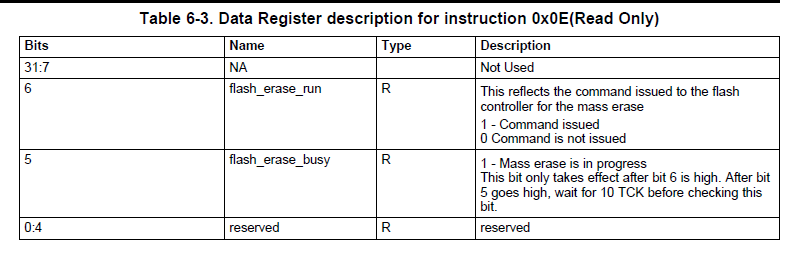
• Do IR scan 001101 (0x0D) followed by IR scan 001110 (0x0E) for ICEPick.

After this step when i scan DR i only receive 0x00 's

is there any error  in these steps.

what should be  the IR and  DR lengths at this stage.

Thanks in advance

  • Hi,

    I sent it to the concerned engineer and they will get back to you ASAP. Please bare with us.

    Thanks,

    PM

  • Please i am Still waiting for the answer. can  someone help me here with the above question

  • Please i am Still waiting for the answer. can  someone help me here with the above question

  • Hi,

    You can use the ROM API for erasing and writing the flash.http://www.ti.com/lit/ug/swru333a/swru333a.pdf

    See if this helps as well (seems to be similar problem):

    Thanks!

  • Hi 

    in my case i cannot use the ROM  API because the device already has a valid flash image in it. so i need to mass erase using JTAG

    and i am also trying the do the same procedure as  described in the below thread

    https://e2e.ti.com/support/wireless-connectivity/zigbee-and-thread/f/158/t/664704

     but  the  solution specified there didnt help in my case

    please let me know the IR and DR length at each step in the  unlocking debug interface

    because i am also suspecting  the issue is related to wrong length.

    The scan lengths i am using  for below steps are mentioned and marked in Blue.

    Scan “Public Connect Sequence (with 0x07 IR(6) followed by 0x89 DR(8))” for ICEPick. Refer to ICEPick
    functional spec for details on “Public Connect Sequence”.
    • Scan “Private Connect Sequence (with 0x1F IR(6)  followed by 0x01 DR(8))” for ICEPick.
    • Do IR scan 001101 (0x0D) (6) followed by IR scan 001110 (0x0E)(6)  for ICEPick.
    • Monitor the status register for 0x0E IR. Look for bits [0:4] & [6] being high and bit [5] being low. When
    this condition is true, the debug unlock sequence is complete.

    At this step i am using a DR scan length of 32.  considering the reference below


    • After the status mentioned above is achieved, issue an ICEPick instruction 111110 (0x3E) to clear the
    debug unlock command.

    Please let me know if something is wrong

    Thanks & Regards

    vinod

  • Hi TI,

    please help me with question. it is a very urgent project for me.

    the delay in the communication is very much annoying.

    please suggest me a better channel of communication.

    Thnx

  • Hi Vinod,

    I have asked our tools team for help with this. Thanks for your patience.

    Regards.

  • Hi,

    thanks a lot for  your support.

    actually below information from the thread you referred has  helped me. i had also to resolve one of my own mistake too

    "The problem was that doing the 0x1F IR scan, the data register selected was a 1 bit register. I didn't know it, it wasn't clearly specified in the documentation. Now it works fine."

    but it is a very pity thing that it is not documented.

    and i also happen to notice one  more thing, when i am trying to flash the CCA area few configuration settings prevent device ACK.

    i tried several use cases and finally understand that it only work without excepting an ACK but there wasn't any documented proof of it.

    ex: when i tried to program the backdoor configuration bit other than FF the device programs it, but does ACK .

    Thanks