This thread has been locked.

If you have a related question, please click the "Ask a related question" button in the top right corner. The newly created question will be automatically linked to this question.

CC1120 with FET booster

Genius 3985 points

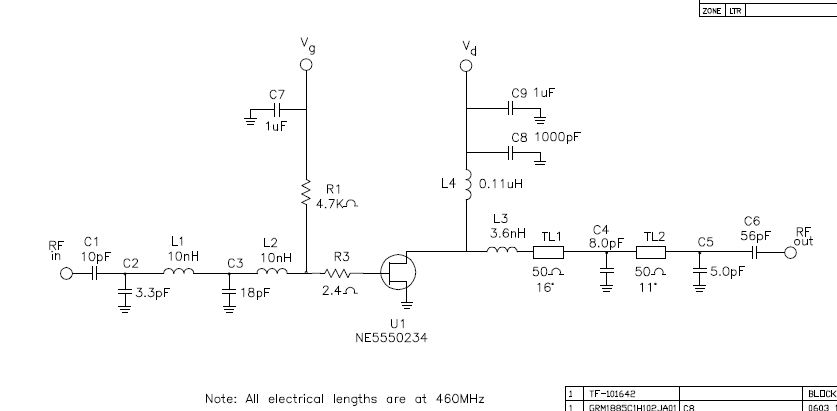
Following a recommendation I've got earlier from Richard, we build up a prototype for 460MHz PA booster.

There is some output (max. 27dB), but we don't reach more regardless what voltage we put on Gate or Drain (only current goes up); expexted is 35dB according to data sheet.
Looking at the harmonics the 1st one is at about 0dB - which is much to high. And only this one is changing when tuning Source/Drain voltage.

The input is either a Marconi generator or an 1120 modul - both don't have that high 1st harmonic.

Any hints what we do wrong?

thx

  • Hi,


    It seems it is compressed at 27dBm.

    What is the device you are using? Could you please post the data sheet?

    Did you get an EV board from the Device Vendor?


    Thanks,

    PM

  • It's a NE5550234-EV04-A, recommened by Richard Wallace in an earlier thread. Richard mentioned, that they tested it and it passed ETSI, so there must be something different in our testbed (as shown just build up in a lab environment); but I don't know where to look.

    The schematic is taken from reference, the TL's are obviously skipped:

  • you cannot skip TL inductors they are there for a reason. Like PM suggested it is best to get an eval board from the vendor and do the validation.

  • I reviewed the data sheet, they provided the Schematic and the PCB Layout.

    You need to follow their layout or Richard layout to get an optimum performance.

    Your layout is not up to the standard and I don't expect the specified performance in the data sheet.

    Thanks,

    PM

  • Good to hear that you are getting 27 dBm output power. What is the input power when measuring 27 dBm out  (gain) ?

    You will need to add some filtering to pass the harmonics.

    Try a 8.2pF in parallel with L3 (3.6nH) to notch out the 2nd harmonic.

    Regards,

       Richard

  • Agree that the TL cannot just be removed since these are acting as inductors in the ref design and the filtering will be effected. If you use some inductance value for the TL then this will also help with the filtering.

    The advantages of using a transistor amplifier are the cost and the biasing / efficiency can be optimized for your application. However, the disadvantage with this compared to an IC PA design is this is much more sensitive to layout and voltage supply variations. The discrete values that are found with your prototype PCB will change when this is used on a different / final layout.

    When the harmonics are suppressed then you will also find then the fundamental output power will increase as well.

    Regards,    Richard.

  • Gents,
    you are right, it's a failure not to recognize the TLs.
    My problem is to transform the reference layout into a 'real-world' application where I don't have more than ~1cm² space for the output circuit. So I need to assume a model for the TL's, e.g. as Richard mentions an inductor (any hint what size we should start with?).

    Also understood, that we need to make the final layout with all the space contraints and leave part values open until we get the PCB samples. Then we have to do some iterations...
    But it makes me wonder that the output doesn't show any kind of e.g. PI-filter to suppress harmonics.

    Some measurements/findings in the current circuit: VGate: 2.8 - 3.3V, below and above that window PA drops and current goes up dramatically if above
    VDrain: 3.3V - 8V : always same PA gain of ~16dB, just current increases when increasing VDrain from ~200mA to 500mA at 8V
    First harmonic (868MHz): ~-3dB, means ~30dB below PA out; second harmonic negligible


  • Hi,

    The area which I used with this PA design was 5.8 x 11.5 mm = 66.7 mm2.

    Layout:

    To start with I would just place 0402 foot holders for the TL parts. I was targeting 20 to 25 dBm output power with 10 dBm input signal at 3.3V. If you are planning for 30 dBm output power then I would add an additional pi-network at the output to surpress the harmonics furthermore.

    What is the RF input power level ?

    To be able determine the optimal biasing for the transistor I would try different gate resistances and add the notch component mentioned previously. Keep the drain voltage as high as possible

    Regards,   Richard


  • For additional support around this transistor I would contact the team at Renesas. The contact I have is a local rep in Sweden: Stefan Carlberg : scarlberg@richardsonrfpd.com

    Regards,

       Richard