This thread has been locked.

If you have a related question, please click the "Ask a related question" button in the top right corner. The newly created question will be automatically linked to this question.

CC2538 balun impedance matching

Other Parts Discussed in Thread: CC2538

I am following the  AN068 for CC2538EM, but I can't get the impedance matching. I would appreciate if someone can tell me what I am missing. 

According to the datasheet, the optimum load is 66 + j64 ohm at RF_P and RF_N. Referring the Figure 7 of the App note (below):

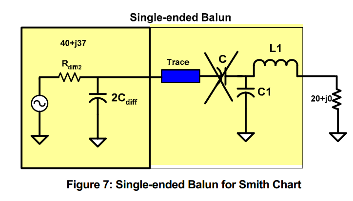
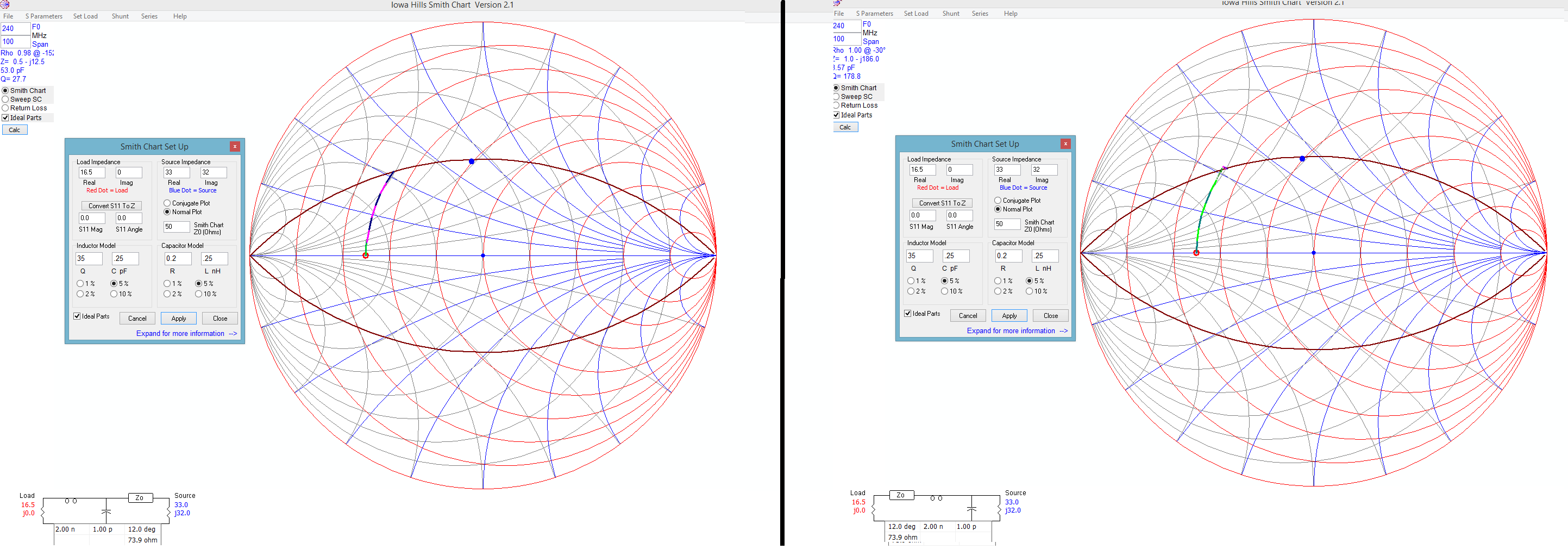
I should have the source part as 33 + j32 ohm and the load should be 16.5 + j0 ohm.  

The copper length from RF_P to L373 (RF pin to sum point of the balun) is approximately 2.564 mm. The copper width is 0.15 mm, copper thickness 35 um,  dielectric thickness to the layer 2 (ground plane) is 0.175 mm. The app note suggests to use 4.1 as dielectric constant, 0.0155 loss tanget.  I add those values into NI's line calculator which outputs impedance as 72.6885 and electrical length as 12.6265 degree

The schematics of CC2538EM uses 2 nH and 1 pF for the balun network. 

I add the values to a Smith Chart as the chapter 6 of the App note does.

step 1: I added the load as 16.5 + j0 ohm (the red circle) and source as 33 + j32 ohm (blue circle)

step 2:  I add a 2 nH serial inductor and 1 pF  shunt capacitor, and then the transmission line with 73.9 ohm and 12 degree (closest possible values on the smith chart program that I use)

As you can see below, source and load is not matched. Do I miss anything on the above calculation or to follow the app note?

  • AN068 is not well written and is a bit confusing. If you remove the chip, terminate the antenna output with 50 ohm and put a differential probe between RF_P and RF_N you should see 66 + j64. This is the impedance where the PA performance is optimal. You will not get close to this number using smith chart and transmission line calculations, if you import the layout into ADS or similar you will get close. Real components have a different transfer function than ideal and parasitics alter the impedance response quite a bit.
  • It explains why I could not get the same smith chart for the board that App note analysis. Thank you for the explanation and the advice.

    One last question about the balun. Is there a high pass and/or low pass filter functionality of the L-C or C-L part  of the balun that is used on the schematics (CC2538 or the one used in the app note)? I wonder if it would cause problem in case I need to use C - C or L-L as long as the impedance is matched? 

  • Not sure exactly which L-C part you are referring to. For CC2538 ref design: C372 and L372/ C382, L381 phaseshift the signal 90 degrees. L373/ C373 is a low pass filter. The two last ones you can change.

    But why do you want to do something else than the ref design?
  • I simulated the circuit on ADS to get the optimum values, then I prepared the new circuit and verified that the problem is solved. Thanks a lot for the very useful information and suggestions.
  • Hi
    How you solved the problem.

    i am facing same issue.

    what should be the differential line impedance from RF pins to matching network.(end point of filter)

    pls. reply
  • Santosh: Please follow the reference design. Why do you want the differential impedance? 

  • Thanks 

    Becuase i am using 8 layer PCB stackup and different pad size

    At least suggest the RF+ pin to End of matching network impedance (single impedance) and same for RF- pin to end of matching n/w (end of filter)

    single ended impedance from RF pin to end of the balun or matching filter?

  • The reason I say use the reference design is that it's not only the impedance but also the filtering that is important.

    Would you be able to have the same distance between layer 1 and layer 2 on your PCB as in the reference design? Then you should be able to follow the reference design.

    See e2e.ti.com/.../943492 for the impedance data.
  • HI

    not same as reference design

    layer 1 to layer 2 distance is 0.15mm

    i can t copied as it is

    I need from RF pin to sum of balun filter impendance values ?
  • If you look at one of my earlier posts in this thread: If you remove the chip, terminate the antenna output with 50 ohm and put a differential probe between RF_P and RF_N you should see 66 + j64
  • remove the chip means remove the CC2538 or remove the inductor and capacitor from filter network

    so what will be single ended impendance.

    i.e. Single ended Impendance value from RF + pin to sum of balun filter end ?
    and vice versa for RF - pin


    Pls share single ended impendance

    is it 33 Ohm ?
  • Hi TER,

    Is 4 port VNA required to do it? How about if one uses a single port VNA and measures the impedance seen through the antenna connector? Would it be a reliable measurement? If it is the case, what values do one suppose to read for RX and TX mode? Do you have any reference values?

  • We have never tried to measure a differential impedance with a VNA due to the potential error sources. The impedance given is typically simulated on our reference design.

    Do you have ADS or similar?

    Our ref design uses 0.175 mm between layer 1 and layer 2. That means that using 0.15 mm will give slightly higher parasitics .
  • Yes, I initially found the matching parameters by ADS, but somehow I have decreased RF performance.

    Are all reference designs purely based on simulations or are they tuned with real life measurements? If it is the case, what measurement tool do you use to tune the boards/antennas?
  • The reference designs are tuned with real life components and all data in the datasheet are actual data measured on our EMs.

    We typically use load and source pull measurements to verify that the optimal match is found.

    If you have used ADS, did the ADS simulations give you the same S11 and S21 (where port 1 is differential between RF_P and RF_N) on the reference design and you design?

    Have you verified your measurement methods by also measuring on a EM?

    Which performance do you see in your design?