
Thank you very much Cynthia.
-Sean
Hello Sean,
The ADS8324 is a single channel device, this is why the device can output the data for the ongoing conversion.
A conversion cycle is made up of two phases, the acquisition phase and the conversion phase. This device takes 4.5 clock cycles…
Hello,
I am working on a design using the ADS8324 converter. For this design I will be operating the device at the full 50kSample/sec rate so I will have to use the 1.2MHz clock source. This application is for a battery operated acoustic…
Hi Henry,
Just to add a little more here, the ADS8324 Is not really characterized to 5V, please take a look at the Power Supply Requirements on page 3 of the datasheet. Also, please take a look at Figure 10. The input is meant to swing +/-Vref around…
Hello,
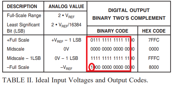
This device used 2s compliment to display the polarity of signal, thus you will need to implement this in the master's method of decoding the output. If a measurement has an MSB of 1, is it negative, and if the MSB is 0 it is positive.
This…
DEARS.
ADS8324 is being tested on the board we designed.
The maximum value of ADS8324 is output up to 1FFF (2^13=8191) and 2.5V.
IN (2.5 to 5V) indicates 8191 only.
How do I read from 0V to 5V?

Thank you
This technical article was updated on July 23, 2020.
Did you know that the input signal might affect how you select the best successive approximation register (SAR) analog-to-digital converter (ADC) for your application?
When we hear the word, “input…


