This thread has been locked.

If you have a related question, please click the "Ask a related question" button in the top right corner. The newly created question will be automatically linked to this question.

C6747's memory map

     I feel confused about C6747's memory map. There are two different addresses of L2 ROM, L2 RAM, L1P RAM and L1D RAM as follows:

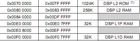
    Why they have two different addresses? What the relationship between them? Can somebody tell me?
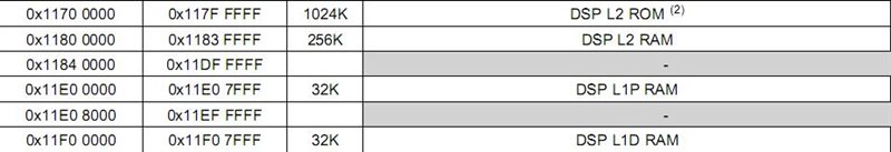


  • wu wu,

    This really should be explained in the datasheet, but I could not find it either. I search for "local" and "global" and neither showed up in this type of explanation. Sorry about that.

    The C674x DSP Megamodule contains the L1 and L2 memories. Only the DSP core can access these memories using the addresses that start with 0x00xx xxxx. These are referred to as Local L2 or Local L1D addresses.

    Other bus masters in the C6747, like the PRUSS and the EDMA3, can access these memories only from the outside using the Global addresses which start with 0x11xx xxxx. Both addresses reach the same physical memory cells, but only the DSP instructions can access the Local address ranges.

    The DSP can also use the 0x11xx xxxx Global addresses with no performance penalty or any negative effect. The only reason not to use the Global addresses exclusively is that some boot modes may be hardcoded to start running at 0x00xx xxxx. This may not be an issue in your application, but just something to be aware of. In all other cases that I can think of, the Global address is the best choice to avoid any later confusion.

    Regards,
    RandyP


    If this answers your question, please click the  Verify Answer  button below. If not, please reply back with more information.