This thread has been locked.

If you have a related question, please click the "Ask a related question" button in the top right corner. The newly created question will be automatically linked to this question.

6713 - HRDY stays high on HPI read

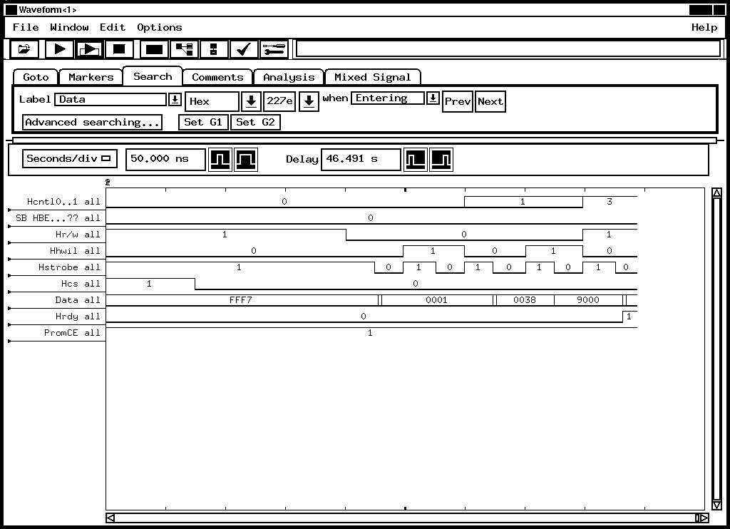
I have a 6713 design where some HPI reads from the CE1 address space (0x9000 0000) cause the HRDY signal to stay high.

All the writes to the HPI from the host (a FPGA is the host side of the HPI) seem to work fine. After writing, I try to read (often from the same address as a write) and some times the read works fine, and sometimes HRDY stays high indefinitely. If I do multiple reads from the same address, I may get one or two good reads in a row then it will fail.

I've looked at signal integrity (on the HDS1 signal) and timing and don't see any questionable issues. The implementation is HDS2 and HAS are tied high and HDS1 is used for the strobe. The protocol, as I read the 6XXX HPI reference guide, is correct, and the same for the good and bad cases.

The only way to clear the HRDY signal after this happens is to reset the DSP. If I restart the DSP and repeat the sequence of writes followed by reads, the behavior is the same.

Any ideas on where to go from here?

  • I have attached a logic analyzer diagram

    The sequence of HPI activity is this:

    1. Take DSP out of reset

    2. HPI write - address 0x180 0000, data 0x0000 3779

    3. HPI write - address 0x180 0004, data 0xF61F 3823

    4. HPI write - address 0x9000 0000, data 0x00F0 00F0

    5. HPI write - address 0x9000 1554, data 0x00AA 00AA

    6. HPI write - address 0x9000 0AA8, data 0x0055 0055

    7 HPI write - address 0x9000 1554, data 0x0090 0090

    8. HPI read - address 0x9000 0038, no data  - this read operation is where the problem starts

  • Can you answer the questions below, so we can have a better understanding of your system?

    • After the HPI writes, can you try verifying through CCS that the writes got written correctly to the memory location?
    • After the first two HPI writes to the configure the EMIF registers, can you try connecting to CCS and see if you can access the EMIF memory correctly through the memory window?
    • Do you see the same HPI read error when you access the EMIF register memory location, 0x180 0000?
    • Do you see the same HPI errors if you write to and read from L2 memory?
    • There are some HPI erratas for C6713, does any of it apply to your silicon revision? 

    --Christina

  • Christina,

    Thank you for the very helpful reply. These questions provoked a lot of discussion and testing. However, we are still not able to resolve the HRDY hanging problem. We are at a loss on how to figure out the problem.

    Here are the answers, I hope that you can provide some more help on where to go from here

    Q: Are the HPI writes......

    A: Yes, the values are shown through the CCS

    Q: After the first two HPI writes...

    A: Yes, the data comes back all F's because the PROM is erased, but the bus cycles look correct

    Q: Do you see the same HPI read error when...

    A: If I loop on reading the EMIF register, I get inconsistent results, sometimes the data is what I expect, sometimes not

    Q: Do you see the same HPI errors if you...

    A: I did not try this because of the erratic behavior of the EMIF register reads

    Q: There are some HPI erratas...

    A: The erratas where checked,  none of known issues seem to target this sympton

    Regards,

    George

  • George,

    Thanks for the responses.  The main reason behind the questions is to have a better understanding on whether the issue is isolated to the EMIF or the HPI. 

    After talking to some additional experts, the HRDY will go low during a read access until the requested data is loaded into HPID.  If data does not get loaded, the HRDY will continue to be high indefinitely.  This can occur when the address being accessed is reserved, or when the EMIF is not configured correctly.


    To determine if this is an HPI bus error, can you try writing to a L2 memory location and then reading back that same memory location? 

    To determine if the HPI is not accessing any reserved memory location, can you try probing the data lines to see if it is sending out the correct address? 

    To determine if the EMIF is configured correctly, after executing the first two HPI writes to the EMIF controller, can you open a memory window in CCS and write another data value into the EMIF memory location?  After writing, can you refresh the memory window a couple of times to make sure that the one memory location remains the same and doesn't affect any neighboring memory location?

    Thanks,
    Christina

  • We tried to write to L2 (0x0001 0000) and then read back.  The bus continued to hang.  We determined that Reset was NOT asserted.  After asserting reset, we have tried to write/read L2 and determined the bus is not being driven by the DSP.  What are the minimum steps to write/read to/from L2?  What are the minimum steps to write/read to/from the EMIF?


  • Kim Volz said:
    We tried to write to L2 (0x0001 0000) and then read back

    Are you using HPI to perform these operations?

    Kim Volz said:
    We determined that Reset was NOT asserted.  After asserting reset, we have tried to write/read L2 and determined the bus is not being driven by the DSP.

    Is this the device reset, or the HPI reset?

    Kim Volz said:
    What are the minimum steps to write/read to/from

    From the DSP side, the code should be very minimalistic.  Most of the programming is done from the host side.  On the host side, you will want to...

    1. Program the HPIC to tell the DSP the type of halfword access
    2. Program HPIA with the desired address. 
    3. Perform read/write operation
      1. Read: read two halfword from HPID
      2. Write: write two halfword to HPID

    More detailed information can be found from the HPI user guide, http://focus.ti.com/lit/ug/spru578c/spru578c.pdf

    --Christina

  • We are using the HPI to perform the read/write operations.  The DSP has power applied and the reset pin is held active low to hold the processor core in reset but allow the EMIF to perform actions required.  The HPI mode is enabled through HD14 (High).  We have tried to multiple configurations with DEVCFG as provided by SPRS186L (p45,46) to insure HPI configuration.

    My question about minimum steps to write/read to/from should have had a better reference.  What hardware and software sequence from 'no power' is required to accompish an L2 write/read? Current steps are:

    Power-Up with HD-14 held High to enter Host Boot mode (SPRS186L p96).

    Maintain Reset to hold core in "stalled" state (SPRS186L p96).

    Write 0x0000000E to DEVCFG to enable HPI.  ( This step has also been omitted. - SPRS186L p45, 46 )

    Write any value to an address in L2 space (0x0000 0000 .. 0x0001 FFFF - SPRS186L p16)  This consists of an HPI transfers as previously defined. The writes have been verified on the logic analyzer.

    Read value back from address. ( This is where the bus gets hung with HRDY being de-asserted (high)).

    Is this a correct sequence?  This processor has been in the field for years, do you have a piece of example code to start this process?

    --Kim


  • Hi Kim,

    just a few ideas...

    the 6713 HPI strobe must be asserted at least 4 CPU cycles, and also de-asserted a minimum of 4 CPU cycles between accesses. In HPI boot mode the PLL will start in bypass mode and the CPU will operate at the CLKIN frequency. At 20MHz CLKIN for example, the HPI strobes must be > 200ns. From your LA screenshot it seems you are using 25ns strobe width, which would require a CLKIN of 160MHz or higher. Is this condition satisfied?

    Another issue I struggeled with some time ago: only the 6713B devices work correctly with strobe width of a 4 cycles. The older devices (without B) require a 10 CPU cycle read strobe.

     -- A. Klemenz


  • Hello A. Klemenz,

    We are running a 40MHz clock so the timing is wrong and we will correct it. 

    We would like a little clarification on the HPI strobe.  The need for 4 CPU cycles between accesses - If we do two writes to L2, between the writes we are required to have 4 HPI strobes?  Is the HPI strobe the only signal required (as in the 6713B is using this as a clocking source)?  Should the extra clocks be 'tacked-on' to the access or preceded the access?

    -- Kim

  • Hi Kim,

    some things are getting mixed-up...

    The 6713 data sheet defines the HPI timing: HSTRB must stay active at least 4 DSP clock cycles = 100ns if the DSP runs at 40MHz. Between HPI accesses an idle time of 4 DSP clock cycles is required, i.e. HSTRB must be de-asserted for 100ns minimum. This idle time is required between *all* HPI transfers, even between first and second half-word transfers. The destination or source memory accessed on the DSP has no effect on this basic HPI timing.

    HPI strobe is not a clock source, it is an asynchronous input. Internally the DSP will synchronize the HPI signals to its clock. This is the reason for the 4 cycle minimum constraint. If you violate this timing the DSP may not recognize the HPI access correctly.

    If your host is an FPGA, the basic HPI timing is easily satisfied with a state machine operating at a suitable clock:

    1. drive HCS = 0, goto 2.

    2. drive HCNTL[1:0], HR/W and HHWIL, goto 3.

    3. write: drive HDATA, assert HDS, goto 4
        read: assert HDS, goto 4

    4: check HRDY: if high stay in 4, else goto 5

    5. write: de-assert HDS, goto 6
        read: read HDATA, de-assert HDS, goto 6.

    6. drive HCS = 1

    -- A. Klemenz


  • Hello A. Klemenz and Christina,

    We have now corrected our timing and are able to get correct read/write to the HPI.  We have more work to test full functionality however, the help that you provided got us past the primary issue. 

    Thank you.

    -- Kim