This thread has been locked.

If you have a related question, please click the "Ask a related question" button in the top right corner. The newly created question will be automatically linked to this question.

TM4C129ENCPDT: Debug Female Connector

Part Number: TM4C129ENCPDT
Other Parts Discussed in Thread: EK-TM4C129EXL

Hi sir,

I have a doubt, 

1. I am using my development board of EX-TM4C129XL as a debugger. So i am going to remove the resistor are R6, R7, R8, R10, R11, R15, R16.Whether it is correct or not?

2. I need JTAG female connector interface with my custom board.but I didnt find it digikey.  Please help me to solve this problem (10 pin 1.27mm pitch)

  • Nishitha

    1. You don't have to remove all the resistors - the debugger will work just fine, if you just remove the jumper that brings power to the main EK's MCU.

    2. You can use connector 3230-10-0103-00, by CNC Tech. Don't forget to get the cable as well.

    Regards

    Bruno
  • Hi Sir,

    Thanks for your reply, 

    Sorry i need some more information clearly, if i remove the ICDI jumper in my development board (EK-TM4C129EXL), so i can able to debug and program my custom board. right?? 

  • Nishita,

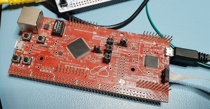
    If you just open JP2 and JP3 you will be able to debug and program an external custom board. This is an actual picture of the same solution, which I was using yesterday.

    Regards

    Bruno

  • Dear Sir,

    Thank you so much, lets try and reply to you 

  • Seemingly removing R40 is must so the ICDI knows the JTAG debug is external, not local.
  • Hi Sir,
    Can i give summary of your answer kindly tell me it is correct or not

    based on your image . i have to use jumper to close that JP2 & JP3 plus removing R40 resistor for debug purpose am i right??
  • BP101 said:
    Seemingly removing R40 is must so the ICDI knows the JTAG debug is external, not local.

    No, it is not. You shall remove R40 when you want to program the TM4C129 MCU using an external Debugger instead of the ICDI emulated by the TM4C123.

    Poster's goal is to use the TM4C123 ICDI as a debugger, to program and debug his own external board.

  • Nishitha Chandrasekar said:
    i have to use jumper to close that JP2 & JP3 plus removing R40 resistor for debug purpose am i right?

    Wrong, wrong and wrong.

    The word "close" means to connect the pins, allowing current to flow through them. If you look closely at the image, JP2 and JP3 are OPEN. The littler jumpers are still visible, but they are inserted in only one pin - I leave them there so not to loose the pieces, that's all.

    As I replied before, there is no need to remove R40.

    The complete schematic for the launchpad is available in this link: http://www.ti.com/lit/ug/spmu365c/spmu365c.pdf 

  • Bruno Saraiva said:
    No, it is not. You shall remove R40 when you want to program the TM4C129 MCU using an external Debugger instead of the ICDI emulated by the TM4C123.

    Schematic states to remove R40 for debug OUT or external JTAG. Why would anyone need or want to use JTAG header with EVM when it has ICDI onboard?

  • I have EVM flashing custom PCB R40 removed using USB port to power ICDI MCU. Did not like the target powering the ICDI which seemed to cause issues with USB port. R40 installed allows debug IN from XDS200 or other debugger.
  • BP101 said:
    Why would anyone need or want to use JTAG header with EVM when it has ICDI onboard?

    If something does not make sense for our needs, it does not imply that nobody else will ever need it... Maybe the person wants to debug the TM4C129 of the EK using an external XDS200 just to see the difference... Maybe he has a complex setup with boosterpacks, and ICDI speed is not enough for his development... Maybe he likes to complicate things...

    Schematics literal statement is: "EXTERNAL_DEBUG pull low to use external debugger to debug the target. Causes ICDI chip to tri-state the JTAG lines". This kind of explains that the ICDI firmware checks this line, and if resistor is not installed, all the JTAG pins of the TM4C123 will become inop...

    The other statement on the same sheet is: "R40 must be removed for debug out. R40 must be instaled for debug in." - that is a confusing sentence that only makes full sense in the mind of whoever wrote it...

    Fact is that you DO NOT need to remove R40 when you want to use the ICDI debugger of the EK-TM4C1294 to program/debug an external custom target. I've been doing that since back when those boards where shipped with XM4C pre-production MCU's...

  • Bruno Saraiva said:
    Maybe the person wants to debug the TM4C129 of the EK using an external XDS200 just to see the difference...

    Your right I actually did use the XDS100 with R40 installed, recall to see if it could work with GUI composer. Later made the EVM ICDI work with GUI.

    Bruno Saraiva said:
    Schematics literal statement is: "EXTERNAL_DEBUG pull low to use external debugger to debug the target. Causes ICDI chip to tri-state the JTAG lines".

    Tri-State the target not the external JTAG is my take, since it also state to remove R40 for debug out. Agree confusing statement to remove R40 for debug out.

    LMFlash works with R40 removed and external JTAG holds pin 3 low high, with R40 installed now recalling LM Flash failed.  

  • BP101 said:
    Tri-State the target not the external JTAG is my take

    Since we don't have (easy) access to the ICDI firmware, we probably won't find out the truth on this one (except if we waste enough time poking those lines with well planned pull resistors...)

    Actually just today I'm using such an EK-TM4C129 board under two different tests: using the EK's TM4C129 as a target, and later, using only the ICDI part to debug an external board. All I do is just remove JP2 and JP3. I do power the custom board externally - using the PC's USB power to drive the Launchpad PLUS the custom board can be risky depending on the external PCB hunger.

    As for the R40... we have never touched the soldering iron there - neither for debugging with CCS nor for just downloading new firmware with LMFlash on the field.

  • Bruno Saraiva said:
    As for the R40... we have never touched the soldering iron there - neither for debugging with CCS nor for just downloading new firmware with LMFlash on the field

    Make since if your JTAG header pin 3 was pulled high or even not connected. The Stellaris RDK had JTAG pin 3 grounded, did the same on our custom PCB.  

  • Hi Sir,
    I have a doubt , for JTAG 1.27mm female connector i got it. but FRC cable is not matching . I bought 1.27mm FRC cable. I dont know how it mismatch could you pls suggest me
  • I do not understand your request. Perhaps you can attach pictures and try to explain what you are looking for.
  • I have not heard back from you. I assume you have resolved your question. If not, please reply with the information requested.
  • hi Sir,

    Sorry for the delay reply. I have bought the FRC connector for 1.27mm. 

    Thanks

    Nishitha 

  • Hi Bruno sir,

    I have removed the JP2 and JP3 connection and using u6 in launchpad connected with my custom . While doing this, it shows an error connection to the target. Kindly help me to do this 

  • Nishitha,

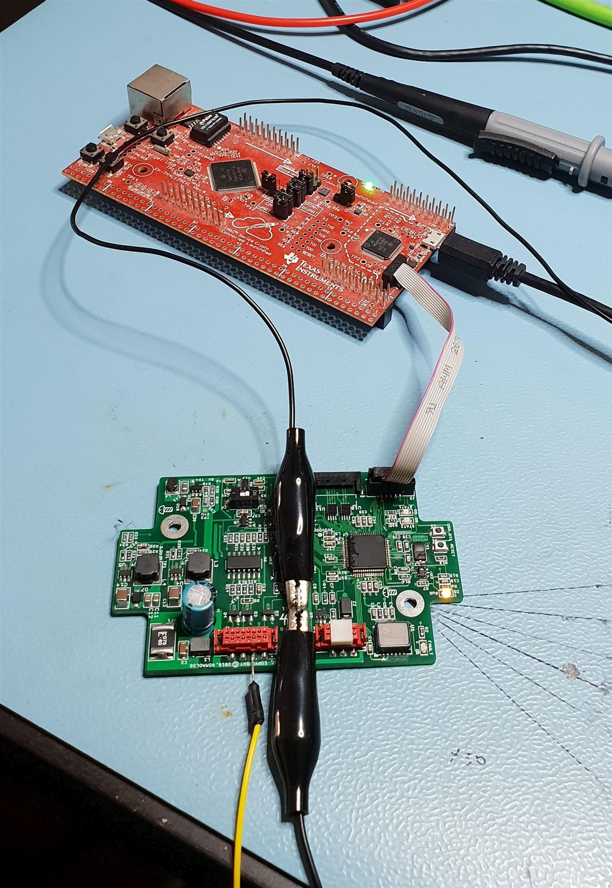
    This is a picture of the lauchpad connected to a custom board. It works perfectly for programming and debugging with CCS.

    If you have an error, it might be a bad cable, something wrong with your custom board, or maybe a CCS/Drivers installation problem (did you select ICDI as your connection on the project properties?)

    Regards

    Bruno

  • Hi Bruno,

    My goal was not to discredit your methods in posts above, rather to suggest odd things can occur with JTAG the way the EKVM U6 header lay out was designed.

    Later after few posts above R40 removal or not, jogged memory had cut JTAG pin 1 3v3 copper trace from powering custom PCB. Trace is very easy to cut between 3v3 VIA and U6 pin 1 for 3v3 from custom PCB so ICDI gets power from computer, not the target

    Not sure why with all the other 0 ohm jumpers pin 1 jumper was omitted. 

    Anyway nice custom PCB above post, any chance U6 pin 3,5,9 tied to DGND?

  • Hi BP,

    Thanks for the input on EMI regarding Tiva related designs - always good to be reminded that there are never enough items of concern when coming up with these boards!

    BP101 said:
    Anyway nice custom PCB above post, any chance U6 pin 3,5,9 tied to DGND?

    Thanks! The best feature of this board is that it works (in a hell of a shaky and harsh environment, might I add). U6 is a RS422 transceiver. Those pins are not tied to GND...

    On the JTAG connector, pin #3 is floating, and 5 and 9 are ground.

    Cheers

  • Hi Bruno,

    Bruno Saraiva said:
    Thanks for the input on EMI regarding Tiva related designs

    Can only hope that some time is spent to update TM4C129 design guide with suggestions to improve SNR perhaps via simple capacitor changes. Charles recently posted an older MCU schematic of EMAC PHY the TM4C1294 had taken design from and VDD caps where parallel mixed values 4.7uf,1nf,100nf,1000nf. The EKXL VDD caps were all 100nf, seemingly RFI/EMI frequency roll off was not considered a problem..   

    Bruno Saraiva said:
    Thanks! The best feature of this board is that it works (in a hell of a shaky and harsh environment, might I add).

    What does it do CNC ? noticed on board regulators and such.

    Bruno Saraiva said:
    ). U6 is a RS422 transceiver

    Funny I was referring to the EVM U6 and pins 3,5,9 on custom PCB end of 10 position cable.  Pin 3 float explains R40 issue at first had to figure out. 

  • Hi Sir,

    Good Afternoon...

    Thanks for your reply. I have done the same method What u have suggested me. Its shows like this 

  • Hi Nishitha,

    You might start by giving more details instead of a single sentence asking for help. What have you done so far to trouble shoot failure and how is JTAG configured in debug properties?

    1. Did the custom board in CCS program load flash the very first time even partially and then fail to connect forever after POR?

    2. That symptom can occur if external XTAL is not functional and application enables MOS after POR.

    3. Please also try LMFlash tool to load your binary application file.