This thread has been locked.

If you have a related question, please click the "Ask a related question" button in the top right corner. The newly created question will be automatically linked to this question.

LMK04832EVM: Desired CLKout at 980MHz and 10MHz while using external SYNC

Part Number: LMK04832EVM
Other Parts Discussed in Thread: LMK04832, LMK04610, LMK03318

Hello,

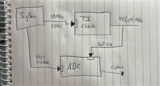
First a little background:

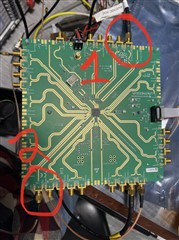
I have your LMK04832EVM board hooked up to a Keysight DSO404A oscilloscope.  I see an output on the CLKout I have selected however there is an offset from the frequency selected on the GUI (TICS Pro) and the frequency observed on the oscilloscope (about 30MHz). 

When I switch the VCO_MUX to CLKin1 and provide an external clock the board I observe the clock buffer (perhaps its the divided external signal frequency) as opposed to what I want to see which is the selected frequency on CLKout.   

Also I need help setting up an external SYNC clock. I'm using an external reference clock at 122.88MHz. The LED for PLL2 is on indicating a lock however the LED for PLL1 is not on and I'm not sure why that is or if that indicates an issue.

What I'm trying to achieve:

My goal is to have two CLKout's, one at 980MHz and one at 10MHz while using the external sync.

If you could share screenshots of the TICS Pro GUI on how to achieve this setup that would be most useful.

Kind Regards,

Alex

  • Alex,

    LMK04832 can't reliably generate 980MHz with internal VCOs. The closest frequency is 980MHz * 3 = 2940MHz, which is 5MHz out of range for VCO1. You must use external VCO or accept that some devices may not be able to lock to the desired frequency due to process variations.

    Also, normally when we talk about SYNC, we're talking about phase SYNC i.e. the ability to align the phase between all outputs arbitrarily. But you describe an external SYNC clock... do you mean a clock to which you will frequency-lock, i.e. the PLL reference frequency? You also mention a 122.88MHz external reference clock, but LMK04832 will have trouble locking to this and producing 980MHz output. Even if the VCO range includes 2940MHz on many devices, the highest suitable phase detector frequency that is a multiple of both 122.88MHz and 980MHz is 160kHz, which will limit the PLL loop bandwidth severely and will greatly elevate the phase noise. LMK04832 PLL1 is designed to operate at lower loop bandwidth and could plausibly lock your 122.88MHz reference input to e.g. a 140MHz VCXO, and the 140MHz VCXO could cascade into PLL2 to provide a higher-frequency reference for the 2940MHz VCO and the 980MHz/10MHz outputs - this would keep PLL2 loop bandwidth high and help reduce the phase noise at the outputs greatly. But 140MHz VCXOs are not very common, and there are no other more common options except at much lower frequency which will negatively impact PLL2 loop bandwidth and phase noise.

    I'm not sure LMK04832 is the right device for this request... between the 122.88MHz external reference clock with GCD frequency of 160kHz, and the required VCO frequency outside of internal VCO range, it seems to me that a different device with a different VCO range or a fractional PLL would be a better fit.

    • What was driving the decision to use LMK04832?
    • What are you clocking that needs 980MHz and 10MHz? Could a different frequency than 980MHz be used to help optimize the frequency plan?
    • Is the 122.88MHz external reference a hard and fast requirement? Could a different frequency be used to help optimize the frequency plan?
    • Could LMK04610 with 5880MHz internal VCO and 120MHz VCXO as a frequency translation stage in PLL1 be a better fit for your application?
    • Would it be easier to use something like LMK03318, with 122.88MHz input, 4900MHz VCO, and a fractional PLL, with N-divider programmed to 39 + 673/768? Is there a phase noise requirement preventing the use of a fractional PLL?

    Regards,

    Derek Payne

  • Hi Derek, 

    Thanks for your reply, please see my responses below, but first I need to correct a mistake.  The output frequency I need is 983.04MHz not 980MHz, sorry about that.  This should be covered by the VCO as 983.04 * 3  = 2949.12.  

    do you mean a clock to which you will frequency-lock, i.e. the PLL reference frequency?

    Here I did mean a phase sync, I want that both signals coming out of the board are in phase.  I thought I needed an external sync (an arbitrary signal coming into the board) to accomplish this.  

    ou also mention a 122.88MHz external reference clock, but LMK04832 will have trouble locking to this and producing 980MHz output.

    The 122.88MHz frequency was chosen because in the LMK04832EVM User’s Guide page 3 says this is the default frequency to be used. 

    What are you clocking that needs 980MHz and 10MHz? Could a different frequency than 980MHz be used to help optimize the frequency plan?

    We will be supplying a 983.04MHz signal to our PLL and then a 10MHz as a sync.  We normally supply our PLL with an external reference clock from a signal generator.  We will be using the LMK04832 in addition as a backup for certain edge cases when we cannot use our external reference clock from the siggen.   

    Is the 122.88MHz external reference a hard and fast requirement? Could a different frequency be used to help optimize the frequency plan?

    No, I only used this as I thought it was a TI requirement for this board.

    Is there a phase noise requirement preventing the use of a fractional PLL?

    Our PN requirement are found in the table below.  I'm not sure if a fractional PLL would be a good fit, moreover now that I corrected myself I think the 983.04MHz goal is within the VCO range and hence shouldn't be an issue.

    Description

    Min

    Typ

    Max

    Unit

    Input frequency


    983.04

    2000

    MHz

    Signal


    Power

    250


    850

    mVppdiff

    Phase noise

    @ 100 kHz


    -129

    -120

    dbc/Hz

    @ 800kHz


    -141

    -138

    dbc/Hz

    @ 5 MHz


    -153

    -147

    dbc/Hz

    >= 10 MHz


    -154

    -150

    dbc/Hz

    Jitter rms


    80

    fs

    Thanks for your support, hopefully my responses provided more clarity.  What would be the order of operations for what I'm trying to accomplish in terms of using the TICS Pro GUI?  Basically an output of 983.04MHz and 10MHz as the SYNC.  The 10MHz is to sync our equipment which can be done one of two ways, preferably we'd like to use the 10MHz signal generated by our siggen and attach this to the sync input on the LMK04832 board.  The other way would be getting a 10MHz signal out of the LMK04832 board and using this to sync our equipment to.  I am unsure about how to set this up using the GUI.  

    Kind Regards,

    Alex

  • Alex,

    Appreciate the clarification, that makes more sense.

    983.04MHz from 122.88MHz is reasonable. However, 10MHz from 122.88MHz would be challenging. The least common multiple of both 983.04MHz and 10MHz is 122.88GHz, so there's no internal VCO frequency that could divide down and output both.

    One thing you could do is provide a 10MHz source (e.g. SigGen, on-board XO) with a 1:2 buffer. One copy of the 10MHz signal can go off-board as a reference to other equipment; the other is provided to PLL1 to lock a 122.88MHz VCXO and subsequently step up to 983.04MHz. An example configuration for LMK04832 is attached below.

    983p04MHz_LMK04832.tcs

    10MHz is particularly challenging to lock on PLL1 when provided from a SigGen or sinusoidal oscillator, because 10MHz sine wave is not high enough slew rate to meet minimum slew rate requirements unless the power exceeds the input buffer absolute maximum ratings (min slew rate = 0.15V/ns; sine wave slew rate at 10MHz = 2π*f*Vpk; Vpk = ~2.4V, Vpp = 4.8V which is well beyond VCC + 0.6V for ESD in both directions). A clipped sine wave source, a squaring circuit, or a high-slew format for the 10MHz signal (e.g. LVCMOS, LVPECL, LVDS) ensures the minimum slew rate requirements can be met.

    Regards,

    Derek Payne

  • Hi Derek,

    Thanks for your help.  I ran the tcs file you sent me however the PLL lock status LED hasn't come on and the output frequency I'm seeing is 1.0332GHz so it isn't locked.  

    One thing you could do is provide a 10MHz source (e.g. SigGen, on-board XO)

    In the sketch below I have our objective (minus the 1:2 buffer for now) and the photo is of our setup.  The red circle with '1' next to it is the external reference clock at 122.88MHz on pin J34 (FBCLKin*_CLKin1*), the red circle next to '2' is our external 10MHz source on pin J45 (SYNC).  I also measured the test point on board for the SYNC and it read 0V.  

    Would you please verify my HW setup is correct?

    Kind Regards,

    Alex

  • Hi Derek,

    I'm worried something might be wrong with the board as even using the default setup under the Default Configuration in TICS Pro the PLL status LED doesn't come on. Perhaps we could schedule a call?

    Kind Regards,

    Alex

  • Alex,

    Apologies for the delay, issue on my end. I see you started another thread so I'll continue discussion over there.

    Regards,

    Derek Payne