

“A clever person solves a problem. A wise person avoids it.” – Albert Einstein
Albert Einstein would have loved analog design – there is always an element of relativity involved. For example, in data acquisition systems, accuracy is relative to your data converter’s reference voltage.
It’s up to the wisdom and foresight of the designer to evaluate the necessary tradeoffs to achieve optimal performance in his or her board level design. We must always consider the gotchas of “under design” in the voltage reference circuitry. Otherwise, your 16-bit data acquisition system could easily perform like a 12-bit system.
Data acquisition systems need external voltage reference circuits when the analog-to-digital converter (ADC) doesn’t include an internal reference. Much to the chagrin of board- and system-level designers, this is often the source of underperformance in precision data acquisition systems. These circuits provide accurate voltages for the ADC from which the ADC’s conversion accuracy is based.
The good news is there are three key components that can help optimize the external reference for ADC performance – the voltage reference, reference drive amplifier and external capacitor. Keep the following tips in mind when selecting these devices:
1) Voltage reference. Look for a reference that suits your overall power requirements with low 1/f (flicker) noise relative to the noise floor of your ADC. If the dominant source of noise is something other than the ADC itself, this will directly influence the precision of your overall design.
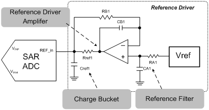
2) Reference drive amplifier. The reference input (REF_in) SAR ADCs contain a capacitive switching network that creates a dynamic current demand on the voltage reference. This can require an external drive amplifier to overcome stability or settling issues between ADC conversions.
Also be sure to consider cap load drive, noise, drift and power consumption in a balanced manner when selecting an amplifier for your application.
3) Capacitor. Even the best low-noise references require a filter to reduce RMS noise to an insignificant level compared to the ADC. Try to keep the noise contribution to more than 1/3 of the ADC RMS noise.
The size of the charge bucket (Cref1) depends on the: 1) average dynamic current drawn from the ADC reference pin, 2) droop requirements between ADC conversions, and 3) amount of current provided by the reference drive amplifier.
For high-precision applications, this value typically ranges from 10-22μF.
These few key considerations should make Einstein proud and help bring a little wisdom – and higher performance – to your next design.
Want to learn more? For a deep dive on how to design the reference circuit, check out TI Precision Design TIPD114, a data acquisition reference design for systems requiring up to 1KHz AC, 1mW, 18-bits and 1MSPS. It’ll come in handy when you’re ready to put this process into calculations.