

Industry 4.0 has revolutionized the manufacturing industry, changing how factories are designed and implemented. In factory automation and process-control applications, Industry 4.0’s impact comes down to two fundamental concepts: the proliferation of decentralized systems and smart deterministic systems. Decentralized systems inherently need to be modular and flexible. Efficient, low-power and thermally optimized designs are the key enablers for such systems. Smart deterministic systems are modules that can detect faults early and increase reliability.
In factory automation and process-control applications, Digital-to-Analog Converters (DACs) are most often found in analog outputs used for both programmable logic controllers (PLCs) and sensor transmitters. In both cases, the DAC can be used to deliver either a voltage output or current output.
The DAC8775 is TI’s newest high-precision DAC, that is the most integrated in the industry by including 4-20mA driver, voltage output and on chip adaptive power management. In this post, I’ll provide examples of design techniques as they relate to the DAC8775 and explore how you can design for the current trends in this industry.
Many system controllers handle hundreds of Input/Output (I/O) points due to the increased number of sensors. This poses a challenge for designers to fit more I/O channels into a small form factor, increasing the need for thermally optimized and highly efficient systems. Most analog output module 4-20mA driver circuits employ a high-side voltage-to-current conversion circuitry with a gain stage. Figure 1 shows a typical architecture.
The loop established by Amplifier A1 converts the DAC output voltage into a current. Through negative feedback, Amplifier A1 will set the voltage across RSET to be equal to the DAC output. This voltage drop across RSET will set the current flowing through the first stage, IM. (I am assuming an ideal case where IRSET is equal to IM.) This generated current, IM, is further gained up by the use of a loop established by the combination of Amplifier A2 and the RMIRROR and RSENSE resistor pairs. The amplifier A2 will force the voltage across RSENSE to be equal to VMIRROR .This generates a load current that is gained up from IM by a factor proportional to the ratio of RMIRROR and RSENSE. RLOAD, shown in Figure 1, usually represents a linear actuator load, as is the case with PLC systems. Since the current passing through RMIRROR is not supplying the load, it will directly reduce the system’s efficiency. A good design practice is to minimize this current – setting it to less than 1% of the output current. For calculation purposes, let’s ignore IM, assuming a high ratio (>1-to-100) between RMIRROR and RSENSE.

Figure 1: High-side voltage-to-current converter
In a typical case, the VPOS voltage can vary anywhere between 12-36V. RLOAD can also vary from a short to 1kΩ. To illustrate the point, consider as our first example the case of VPOS equal to 36V and RLOAD equal to 1Ω. When a valve is set to full scale, the controller will drive 20mA through the load. This means that the power consumed by the load is PLOAD = I2R = 0.4mW.
The total power generated is Pgenerated = VI = 0.72W. From this example, it’s evident that the voltage-to-current conversion circuitry dissipates the rest of the power: 0.72W-0.4mW = 0.7196W. This is a highly inefficient system and will cause an unnecessary increase in system temperature.
Consider a second example where the load impedance is higher, at 1kΩ. In that case, PLOAD = I2R = 0.4W. The total power generated is Pgenerated = VI = 0.72W. The voltage-to-current conversion circuitry dissipates the rest of the power: 0.72W-0.4W = 0.32W.
You can imagine that adding more channels in such a small space becomes unsustainable if there is a vast amount of power loss, which directly increases system temperature, reduces reliability and increases failures. The examples I’ve given show the power loss just for a single-channel design. In the case of four channels, the power losses in the first and second examples would be close to 2.8W and 1.2W, respectively.
Because power loss increases dramatically with the use of even higher channel count modules, one possible solution is to adaptively change the VPOS supply depending on the load. You can do this by adding a simple feedback network and employing a buck/boost converter to supply just the necessary power to the load. Such a system would look like the block diagram shown in Figure 2.
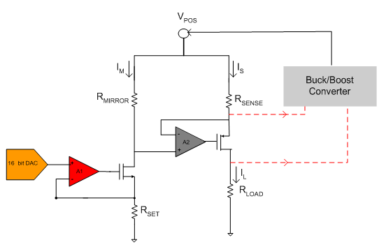
Figure 2: High-side voltage-to-current converter with a buck/boost converter
In this design technique a buck/boost converter will sense the drain-to-source voltage of the output FET driving the load and generate an internal proportional error current. Through a complex state machine algorithm the device will make a decision to buck or boost the supply. This technique is utilized in the quad Channel DAC8775 to achieve higher efficiency.
If you use the same values as the first example, when the load is 1Ω, the buck/boost converter would buck the supply to the DAC down so that it gets the minimum supply needed. In the case of the DAC8775, that would as low as 4.5V.
As in the first example, PLOAD = I2R = 0.4mW. The total power generated is Pgenerated = VI = 0.09W. The voltage-to-current conversion circuitry dissipates the rest of the power: 0.09W-0.4mW = 89.6mW. Therefore, the power consumption is improved by a factor of eight when compared with example 1.
For the 1kΩ load case, PLOAD = I2R = 0.4W. The total power generated is Pgenerated = VI = 0.46W, since the buck/boost converter will set VPOS to 23V. The voltage-to-current conversion circuitry dissipates the rest of the power: 0.46W-0.4W = 0.06W. Therefore, the power consumption is improved by a factor of five when compared to the design with no buck/boost converter feedback.
The DAC8775’s efficiency also results in a much more thermally optimized system. Comparing the junction temperature of the die in a four-channel design with and without adaptive power-feedback circuitry shows a significant improvement in die temperature. Figures 3 and 4 show measurement results for the DAC8775, comparing the die temperature with and without the use of a buck/boost converter for both 1Ω and 1kΩ RLOAD cases. As you can see from Figure 3, this technique can improve the junction temperature by up to 36°C.
When squeezing more and more channels into a smaller space, thermal optimization becomes a critical performance parameter that differentiates module capability. In thermally unoptimized modules, system failures are common and performance degradation occurs due to large temperature drift. The DAC8775 addresses both of these challenges due to its high integration and high efficiency and achieves excellent DC and drift performance.
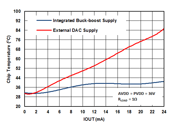
Figure 3: Die temperature for RLOAD of 1Ω

Figure 4: Die temperature for RLOAD of 1kΩ
In case the die temperature goes above 150°C, the DAC8775 offers an over-temperature alarm, part of an extensive set of smart diagnostic features that help detect faults early. These include open load, short circuit, cyclic redundancy check (CRC), watchdog timer and compliance voltage. In addition to fault alerts, the device allows you to choose pre-set actions that facilitate reliable system operation. You can tell the device to do nothing, shut down or go to a pre-programmed safe code.
TI’s wide portfolio of signal-chain offerings enables you to design modules that are efficient, thermally optimized and smarter. Learn more by checking out TI’s broad precision DAC portfolio or the DAC8775.
Additional resources
- Download the DAC8775 datasheet.
- Evaluate the DAC8775 with the DAC8775 evaluation module.
- Download the reference design, “EMC/EMI tested Quad Channel Industrial Voltage and Current output driver reference design.”
- Download the reference design, “Less than 1W, Quad Channel Analog Output Module with adaptive power management reference design.”
- Learn more about TI’s precision data converter portfolio.
- Watch this video about the DAC8775 features and uses.