

In this post, I’ll show how to design a cost-optimized, discrete, wide-bandwidth instrumentation amplifier using the TLV3544. Instrumentation amplifiers are used for their high input impedance and ability to convert differential voltages to single-ended voltages. Fast current sensing, precision data acquisition, vibration analysis, microphone pre-amplification, ADC drivers and medical instrumentation are all applications that need instrumentation amplifiers with wide bandwidth.
TLV354x devices provide a rail-to-rail input/output, 200MHz unity gain bandwidth (GBW) and 150V/µs slew rate, which is designed for the applications I just mentioned. Figure 1 shows the standard three-operational amplifier (op amp) topology.
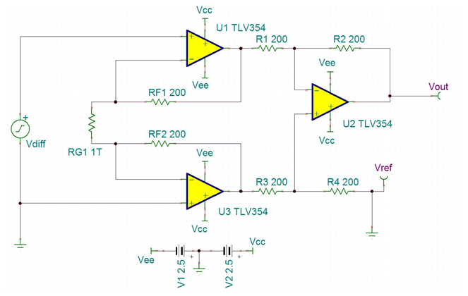
Figure 1: Discrete three-op-amp topology using the TLV3544
The input stage uses dual noninverting amplifiers that enable high impedance at both inputs, whose gain is defined by RF1 = RF2 and RG1. The output stage consists of a difference amplifier with a low impedance output, whose gain is set by R2 = R4 and R1 = R3. The reference voltage, input stage gain and output stage gain define the output voltage, shown in Equation 1:

Note that the tolerance of the resistors in the instrumentation amplifier will negatively affect the CMRR and gain error of the circuit. That is why there is a cost and performance trade-off between discrete and integrated instrumentation amplifiers.
The bandwidth of instrumentation amplifiers is bounded by three characteristics: the open-loop gain (Aol) of the op amp, the noise gain (Gn) and filtering. Both Aol and Gn are covered in the TI Precision Labs training series on bandwidth (see part 3, “TI Precision Labs – Op Amps: Bandwidth 3” – viewing requires a myTI login). The output-stage difference amplifier’s noise gain determines the circuit’s bandwidth.
The TLV3544, like many high-speed amplifiers, will have stability issues if the feedback resistors are too large. Figure 2 simulates the effects of 200Ω feedback resistors versus 500Ω feedback resistors. Note that 45 degrees of phase margin (PM) is necessary for stable operation. Increasing the resistor values allows for lower power consumption and larger RG1 values to set the gain.
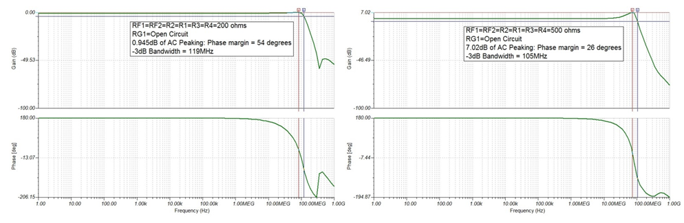
Figure 2: TINA-TI™ software frequency response showing AC peaking, PM and bandwidth with 200Ω (54 degrees PM) versus 500Ω (26 degrees PM) feedback resistors
Since the instrumentation amplifier is discrete, you have access to the feedback paths, which allows you to compensate for AC peaking. By placing capacitors in the feedback path, you introduce multiple poles that create a low-pass filter and attenuate the peaking. Equation 2 calculates the -3dB frequency (fp) of this low-pass filter:

Figure 3 shows the schematic and frequency response. Remember that adding a filter will affect the overall bandwidth of the circuit.

Figure 3: TINA-TI software schematic and frequency response of compensated feedback paths
Since this instrumentation amplifier topology only requires three op amps, the fourth op amp provided by the TLV3544 can serve as a reference buffer for single-supply systems or as an integrator for high-pass filtering of the input.
Thus, you can use the TLV3544 to make a discrete wide-bandwidth instrumentation amplifier that is ideal for cost-optimized, high-precision, wide-bandwidth applications.
Have questions or comments about other design considerations for discrete instrumentation amplifiers? Log in and leave a comment.
Additional resources
- Watch more than 40 on-demand videos about topics such as bandwidth and stability on TI Precision Labs.
- Read Pete Semig’s blog series on VOUT vs. VCM limitations, “Instrumentation amplifier VCM vs. VOUT plots: part 1, part 2, part 3,” to avoid common pitfalls when using instrumentation amplifiers.
- See TI’s portfolio of performance op amps for cost-conscious applications.
- Find commonly used analog design formulas in our wildly popular and free Analog Engineer’s Pocket Reference e-book.
- Read more blogs about precision amplifiers.
- Learn about TI’s entire portfolio of amplifier ICs and explore technical resources.
-

Cole Macias
-
Cancel
-
Up
0
Down
-
-
Reply
-
More
-
Cancel
Comment-

Cole Macias
-
Cancel
-
Up
0
Down
-
-
Reply
-
More
-
Cancel
Children