Have you ever wondered why a traditional 3-op amp instrumentation amplifier’s offset voltage changes with gain? Figure 1 is an excerpt from the INA333 datasheet that shows an example of the dependence of the offset voltage on device gain. Today, let's walk through how the equation is determined.
Figure 1: INA333 offset voltage specification
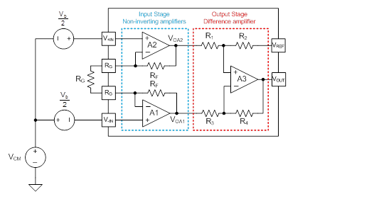
Traditional 3-op amp instrumentation amplifiers have two stages. The input stage consists of two non-inverting amplifiers that buffer (or amplify) the differential input signal. The output stage consists of a difference amplifier that converts the differential signal to a single-ended output. It also provides the ability to add a reference voltage to the output. Figure 2 depicts a traditional 3-op amp topology.
Figure 2: Traditional 3-op amp instrumentation amplifier
Given GDA and GIS are the gains associated with the difference amplifier and input stage, respectively, Equation 1 is the general transfer function of the circuit in Figure 2 (assuming R2=R4 and R1=R3).
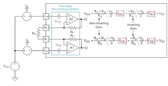
Each op amp in the instrumentation amplifier has an input offset voltage. The offset voltages associated with A1 and A2 are amplified depending on the ratio of RF and RG. Modeling the input offset voltage as voltage sources in series with each non-inverting terminal of A1 and A2 yields output equations as shown in Figure 3.
Figure 3: Output of A1 and A2 with offset voltage model
An intuitive way to look at the equation for VOA2 in Figure 3 is that the sources in series with the non-inverting input are amplified by the non-inverting gain of A2. The sources in series with A1’s non-inverting input are essentially connected to A1’s inverting terminal, which ultimately add to A2’s output after being gained by A2’s inverting gain. Performing the same analysis for A1 yields the equation for VOA1.
Equation 2 shows the equation for VIN-DA, which is the difference amplifier’s input voltage (Figure 4). Notice that the input stage offset voltages are amplified by the gain of the input stage, GIS, as defined in Equation 1.
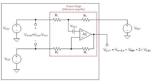
Figure 4 depicts the output stage difference amplifier with the offset voltage model. The gain of the difference amplifier is set to 1V/V, which is consistent with most instrumentation amplifiers. We see that the offset voltage, VOS3, appears in the output equation. It is amplified by 2, which is the non-inverting gain of A3.
Figure 4: Difference amplifier with offset voltage model
Since the gain of the difference amplifier is fixed, the offset contribution of A3 cannot change with gain. Therefore, we can represent the offset voltage that appears at the output (referred-to-output, or ‘RTO’) of the instrumentation amplifier as shown in Equation 3, where GIS is the gain of the input stage, VOS_IS is the net offset voltage of the input stage and VOS_DA is the offset voltage of the difference amplifier stage.
Even though Equation 3 appears the same as the offset shown in Figure 1, it is not! Looking carefully at Figure 1 shows that the parameter is “Offset Voltage, RTI” which means the offset voltage is referred-to-input. Equation 3 must be divided by the gain in order to refer the offset voltage to the input, as shown in Equation 4. Equation 4 corresponds to Figure 1.
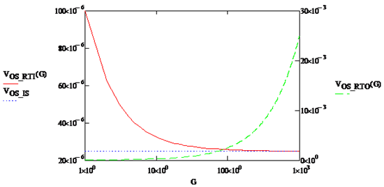
Figure 5 is a plot of the input stage and overall instrumentation amplifier offset of the INA333 (referred to the input). Notice that in a gain of 1 V/V, the offset of the instrumentation amplifier simplifies to VOS_IS+VOS_DA (25µV+75µV=100µV). As the gain increases, the offset voltage approaches VOS_IS (25µV). Referred to the output, however, the offset voltage increases with gain, as expected and shown by VOS_RTO in Figure 5.
Figure 5: Plot of VOS_RTI & VOS_RTO vs. Gain for INA333
In summary, remember that the offset voltage specification is referred-to-input and must be multiplied by the gain to determine its contribution at the output, as shown in Equation 5.
(Note: Please click on each image to enlarge.)


