

It’s simple to design a multiplexer (or mux for short) into a signal chain, right? After all, the device simply funnels multiple signals into a data converter.
In reality, a mux can significantly impact the performance of a signal chain in a variety of ways. For example, the on-capacitance can cause crosstalk between channels. Signal- and temperature-dependent variations in the on-resistance can introduce signal distortion. Together, the capacitance and resistance of the mux can limit signal bandwidth. Charge injection can introduce transient errors when the mux switches channels and impact settling time at the output.
To optimize signal-chain performance, it is important to understand these examples as well as numerous other ways that a mux can impact a signal, especially because multiplexers are optimized for different performance characteristics, and thus for different applications. Figure 1 is an example circuit containing a mux with its output connected to an inverting operation amplifier (op amp).
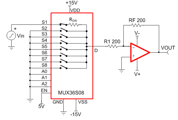
Figure 1: A mux connected to an inverting amplifier introduces gain error
This circuit is one of many common mux configurations in a signal chain, but as we will discover, this design will lead to significant signal gain error. Assuming that the op amp is ideal (no offset, bias current, input/output limitations, etc.), Equation 1 expresses the signal gain as:

Because the MUX36S08 is not an ideal mux and has internal capacitance as well as an on-resistance of 125Ω, Equation 2 expresses the effective gain of the system as:

The calculated signal gain in Equation 2 poses a huge problem if the output of the op amp is connected to a data converter designed to receive the full gain, as nearly 40% of the converter’s range would not be utilized. This equation doesn’t even take into account the on-resistance variation that occurs from changes in temperature, signal voltage or the voltage applied to the supplies.
Figure 2 shows one of the on-resistance curves for the MUX36S08. You can see that the resistance changes based on the temperature as well as the applied signal (the source or drain voltage). The curve that results from changing the signal voltage is known as on-resistance flatness, which can introduce nonlinearity and gain variation. Subjecting the circuit in Figure 1 to a full ±18V sinusoidal signal and temperatures from -40°C to 125°C, the on-resistance of the mux can vary from approximately 75Ω to 250Ω, resulting in an effective gain ranging from -0.44 to -0.73.

Figure 2: On-resistance vs. source or drain voltage
Luckily, you can effectively ignore the on-resistance of the multiplexer through very simple design precautions. Figure 3 shows the output of the mux connected to an op amp configured as a buffer. The high input impedance of the op amp eliminates any gain error the system would otherwise experience.

Figure 3: A mux connected to a buffer effectively eliminates gain error caused by the mux on-resistance
As a reminder, the effect of on-resistance on signal gain is only one of the many ways that a multiplexer can impact the performance of a system. When you’re ready to learn about the other ways a mux can add error and distortion to a signal as well as how to mitigate the impact a mux has on signal chain performance, check out the new TI Precision Labs training series covering multiplexers.
Additional resources
- Explore more than 40 hands-on trainings and lab videos from TI Precision Labs.
- Read a blog about whether a low-leakage multiplexer really matters in a high-impedance PLC system.