

Monitoring the voltage level of a coin cell in a portable device or in back-up service is a common, simple application for modern CMOS operation amplifiers (op amps).
Figure 1 shows an implementation using the 1.8-V, OPA333 zero-drift op amp. The coin cell has a voltage of 3 V, while the circuit is powered by a 3- to 5-V level.
Oddly, I’ve had customers report that the circuit drains the coin cell long before the expected life; in just a matter of days, or even hours! These customers found when the op amp was removed, the coin cell remained charged. That piqued my curiosity, and I began an investigation to find out what was happening.
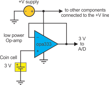
Figure 1 - OPA333 unity-gain amplifier connected to monitor coin cell voltage
A popular coin cell, the lithium CR2032, is rated at 175 mAh capacity and 200 uA continuous current. The OPA333 input bias current is typically 70 pA. That alone wouldn’t deplete the cell for years. Something else was draining the battery. A close look at the OPA333 internal schematic revealed a plausible discharge scenario.
Figure 2 shows a block diagram of the amplifier core and its input ESD protection. Remember that most ICs are protected against ESD during out-of-circuit handling. The ESD cells are designed to be off under normal operating conditions.
The OPA333 ESD input protection has low-leakage steering diodes connected from each input, to the supply lines. An ESD clamp connects between those lines. These diodes are normally reversed biased. However, if the supply voltage V+ is turned off, becoming high impedance, diode D3 can become forward biased. Then, the amplifier core and anything else connected to V+ can drain current from the coin cell.
The OPA333 quiescent current is only 17 uA, so it is probable other components connected to the +V supply line were drawing current too.

Figure 2 - Internal block diagram shows current path through D3 from the non-inverting input to +V supply line
Some op amps have a shut-down pin. When in that mode, they draw a tiny amount of supply current. However, if the ESD cell uses the Figure 2 design, the diode can still conduct current.
The solution is to employ an op amp with a different ESD cell design.
Figure 3 shows the ESD cell design used in the TLV2450 rail-to-rail input/output op amp. It uses a fast, low-leakage clamp - similar to a zener diode. It turns on fast and limits applied voltages to a safe level during an ESD event. There is no internal current path to the VDD pin.
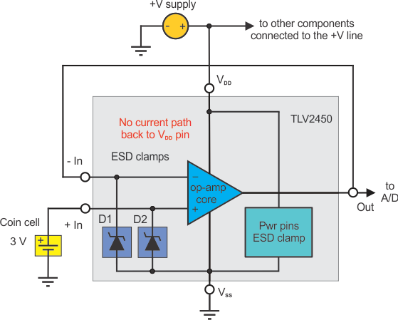
Figure 3 - The TLV2450 uses an input ESD clamp. There is no internal current path from the input to the VDD pin.
It may be difficult for an engineer to determine the ESD cell design an amplifier uses. One hint can be found in the amplifier’s data sheet. When you look at the Absolute Maximum Ratings, if the signal input has a range listed, such as -0.3 V to (V+) + 0.3 V, the 0.3 V is a limit that assures the ESD diodes remain off. Any higher, and they may turn on.
If in doubt, visit our Precision Amplifiers Forum here in the E2E™ Community and submit a question. One of our Applications Engineers will research it for you.
-

Thomas Kuehl
-
Cancel
-
Up
0
Down
-
-
Reply
-
More
-
Cancel
Comment-

Thomas Kuehl
-
Cancel
-
Up
0
Down
-
-
Reply
-
More
-
Cancel
Children