
This technical article was updated on July 23, 2020.
High-precision data-acquisition systems are designed to minimize errors from various system components, like those introduced by switching transients on the reference input of a data converter. In the case of a successive approximation register analog-to-digital converter (SAR ADC), circuitry inside the data converter as it connects and disconnects different capacitive loads throughout the conversion cycle causes switching transients. Other data converters, such as delta-sigma ADCs and digital-to-analog converters (DACs), can also impose switching transients on the reference pin.
A simplified representation of the SAR ADC architecture is shown in Figure 1. During operation, switches S1 and S2 inside the ADC control the acquisition and conversion cycles. When S1 closes and S2 opens, a transient condition occurs on the input because of an impedance change. There are detailed technical resources that discuss how to optimize the input circuitry to minimize the impact of the input transient, such as the user guide for the TI Design TIPD173, which showcases a 16-Bit 1MSPS Data Acquisition Reference Design for Single-Ended Multiplexed Applications. But in this post, I’d like to focus on the transients generated on the reference voltage input pin (VREF) since these transients and their effect on system performance are often overlooked in system-level design.

Figure 1: Simplified SAR ADC internal architecture
The VREF pin of a SAR ADC is internally connected to a capacitive DAC (CDAC), highlighted in red in Figure 1. Figure 2 provides additional detail on a simplified CDAC structure. The CDAC is a binary weighted capacitor array that determines the digital value that best matches the input voltage in comparison to a reference voltage. The key point is that the reference input pin connects to the binary weighted capacitor array, which can cause variations in the reference voltage applied to the VREF pin during a conversion cycle. The capacitors in the array will not be at the same potential as the reference, so there will be a large, fast spike of in-rush current when connecting the capacitors to the external reference.
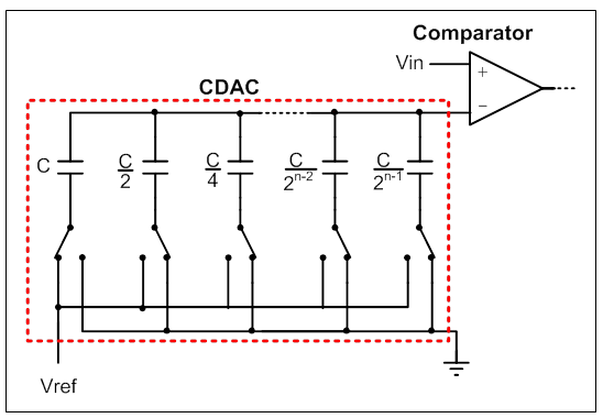
Figure 2: The internal CDAC architecture results in a switched capacitor load
Figure 3 shows the spikes in reference input current that occur throughout the conversion cycle, which can be as large as 10mA and very short in duration (nanoseconds).
![]()
Figure 3: Switching transients on the VREF pin of a SAR ADC
For optimal accuracy, the voltage reference connected to the SAR input needs to respond to the large, fast current spikes. These fast-switching current transients can cause a voltage drop across the high output impedance of the voltage reference. This voltage drop directly affects the output voltage of the reference and therefore the input voltage to the VREF pin of the ADC, resulting in erroneous conversion of the input signal by the ADC.
To minimize the error introduced by these switching transients, the voltage reference should resettle to the desired output voltage between each current spike. A stand-alone voltage reference is designed to deliver a very accurate and stable voltage, given that the load is very light and slow-moving. Since these current spikes are very short in duration and large in magnitude, the reference is often buffered with a high-speed operational amplifier (op amp) (see Figure 4). In addition, placing a capacitor at the pin can provide the total instantaneous current needed.
Although high-speed op amps are good from a transient perspective, they generally are not optimized for DC accuracy, such as offset voltage, linearity and drift. Thus, it can be challenging to find a buffer that meets the DC accuracy requirement but also has good transient behavior. In some cases, an amplifier topology containing two amplifiers will achieve this challenging objective. The data acquisition reference design user guide that I mentioned earlier explains this topology in more detail and covers the selection of the voltage reference, buffer amplifiers and associated filter components.
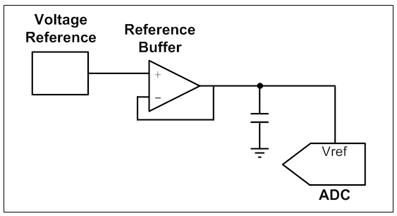
Figure 4: Voltage reference circuit using a high-speed amplifier
In order to simplify the system-level design efforts required to minimize the effects of switching transients on the reference pin, TI’s REF6000 voltage reference family integrates the reference buffer with the voltage reference. Figure 5 shows this integration in a simplified data-acquisition system. The internal buffer is optimized to respond well to the types of transients generated on the reference pin of a data converter and is also optimized for DC performance. In addition, this combination reduces circuit board area, as it combines the voltage reference and reference buffer.
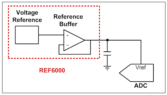
Figure 5: Voltage reference circuit using an integrated voltage reference and reference buffer
With this integrated approach, the performance of the ADC improves by providing a high-bandwidth, low-output impedance, DC-optimized solution for the input to the VREF pin. Table 1 compares the noise and distortion performance of an ideal ADC to ADCs with different voltage reference circuit configurations. You can see that the case without a reference driving buffer has degraded performance. Comparing the integrated reference buffer to the external buffer, the reference with the integrated buffer performs best.
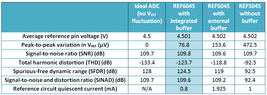
Table 1: ADC performance of various buffer configurations with an 18-bit ADC sampling at 1MSPS and 10kHz input frequency
It’s important to consider the design of the voltage reference circuit when designing a high-precision data-acquisition system. One way to improve overall system performance is to optimize the driving buffer that handles the fast switching transients of the data converter in order to reduce distortion and error. We’ve taken care of that for you by integrating the reference buffer and voltage reference with TI’s REF6000 family of voltage references.
Be sure to subscribe to Precision Hub by clicking that option in the upper right corner of this page to receive design advice about voltage references and more right to your inbox.
Additional resources
- Read the white paper, “Voltage-reference impact on total harmonic distortion,” for a more detailed discussion about the impact of reference loading on distortion.
- See TI’s broad range of voltage references, such as the series voltage reference portfolio featuring the REF6000 family.
- Learn more about the REF6025 2.5V output high-precision voltage reference with integrated high-bandwidth buffer and family of related output voltage variants.
- Learn about TI’s data converter portfolio and find technical resources.