Because of the holidays, TI E2E™ design support forum responses will be delayed from Dec. 25 through Jan. 2. Thank you for your patience.

This thread has been locked.

If you have a related question, please click the "Ask a related question" button in the top right corner. The newly created question will be automatically linked to this question.

[FAQ] J784S4XEVM: How to enable second PCIe slot for two SSD cards

Part Number: J784S4XEVM

By default, the second PCIe slot is not configured for PCIe root complex mode from the SoC-side, meaning if we wanted to connect an end point device like a NVMe SSD card, the link does not go up.

When connecting a NVMe SSD card to the second PCIe slot J17 which is connected to 2 lanes of PCIe, boot logs reports "Failed to init phy". Link for PCIe is only initialized on the first PCIe slot in J14, which is connected to 4 lanes of PCIe.

  • NOTE: This FAQ will be applicable for 8.6 SDK or older. For 9.0 SDK and onwards, a patch is integrated into SDK to provide internal refclk to PCIe slot, so this hardware mod should not be needed.

    This is an extension of [FAQ] TDA4VM: TDA4VM/DRA829V: routing PCIE reference clock externally with pictures and example of why PCIe reference clock needs to be routed externally.

    When using the 8.6 SDK release of J784S4, no software changes to device tree are needed to enable second PCIe slot for PCIe RC mode (aka the mode where SSD cards can be connected to the PCIe slot to be used as a second storage device).

    However, only hardware modifications is what is needed to make both PCIe slots to act the same way. As shown in below schematic, for the second PCIe slot, R155 and R152 are "DNI" or "Do Not Install" so by default CLKGEN_PCIE1_2L_REFCLK_P and N (the external clock) is not connected to CON_PCIE1_2L_REFCLK_P and N (the PCIe connectors).

    1. R169, R168, C129, and C125 need to be removed and stored.
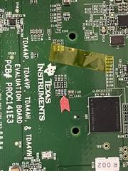
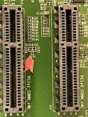
    2. R155 and R152 need to be connected (this can be done by physically "rotating" C129 and C125 to the R155 and R152 position) to connect external clock to PCIe connector.
    3. R169 and R168 should not be connected to R171 and R170, since the SOC_SERDES0_REFCLK_P is already connected to the SOC's internal clock by default, and connecting to external clock could cause contention between the clocks.

    Refer to below images for how the resistors should physically look on the board after the changes have been made:

    And result of these hardware changes would be two PCIe cards like NVMe SSD cards that can be used as storage. Attached is a video of two SSD cards doing read/writes simultaneously connected to the top two PCIe slots J14 and J17.

    IMG_1084.zip

    For reference, similar information can be obtained by referencing schematic files https://www.ti.com/lit/zip/sprr458 of each J7x platform. And these are usually found on the product page of the EVM https://www.ti.com/tool/J784S4XEVM.

    Additional reference can be found in user guide referring to second PCIe slot needing external clock and reasoning for why the board modification is needed:

    As a note: If the link is still not coming up, please make sure the SSD cards are NVMe SSD cards, and they have been formatted and partitioned for ext4fs (Linux filesystem).