This thread has been locked.

If you have a related question, please click the "Ask a related question" button in the top right corner. The newly created question will be automatically linked to this question.

VCA824: Basic question

Part Number: VCA824

Hi,

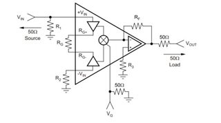
I would like to ask you a basic question about the circuit of Fig76, datasheet 29page.

There are 2 input registers in the circuit, R2/R3.

I think that the input registance of VCA824 is set by the registers.

Will you tell me how to select the value of the registers?

If we would like the input registance be max, we should remove the registers (R2/R3), I suppose...

I would like to know the role of R2/R3. (Except impedance maching..)

Sorry for my basic question.

Thank you for your support.

  • Hello Suzuki-san,

       This device is voltage controlled variable gain amplifier rather than a programmable gain amplifier. Therefore, there is no digital interface (registers) or gain control bits. The maximum gain is set by external resistors using the pins +RG and -RG (2V/V to 100V/V). The gain range (40dB) is controlled by an external analog voltage which is set by the VG pin. Section 8.4 goes into more detail for gain functionality for this device, and datasheet Figure 13, Figure 35, and Figure 56 for graphs on the gain vs gain control voltage.


       The only purpose of the input resistors (R2/R3) is what you have already stated which is simply impedance matching, as well as keeping the inputs impedance balanced. Since, the gain set resistor is connected between the two input buffer output pins, the input impedance is independent of the gain settings.

    Thank you,

    Sima 

  • Hi Sima-san,

    Thank you for your reply !

    I understood.

    Best Regards,

    Takumi