This thread has been locked.

If you have a related question, please click the "Ask a related question" button in the top right corner. The newly created question will be automatically linked to this question.

OPA192: Transimpedance amplifier issue

Part Number: OPA192
Other Parts Discussed in Thread: OPA392, TINA-TI, OPA380, OPA4192, OPA2192

Hi Forum,

I am currently looking at improving the existing Photodiode circuitry to measure light at low levels (close to 0.01 Lux).I can understand the complexities of measuring light at these levels, however this is not what I am after. 

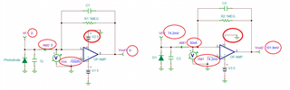
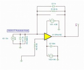
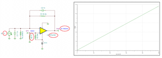
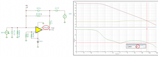
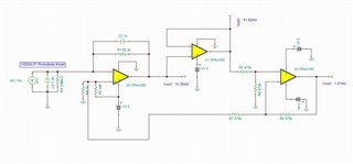
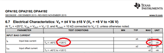
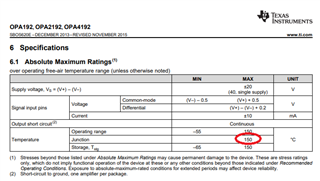
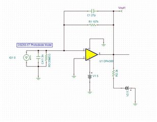
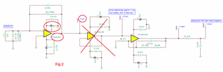
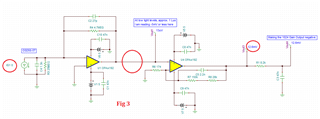
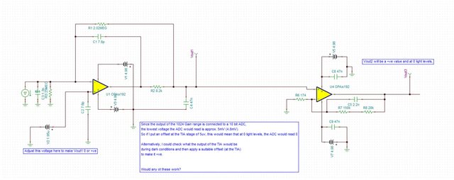
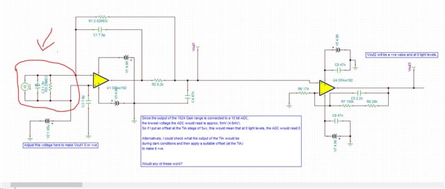
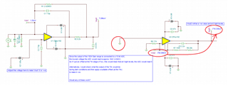
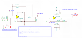
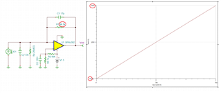
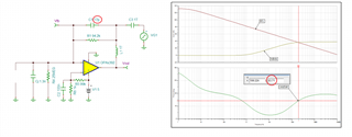
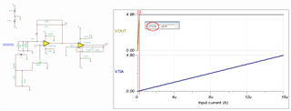
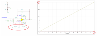
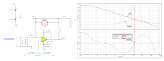
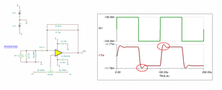
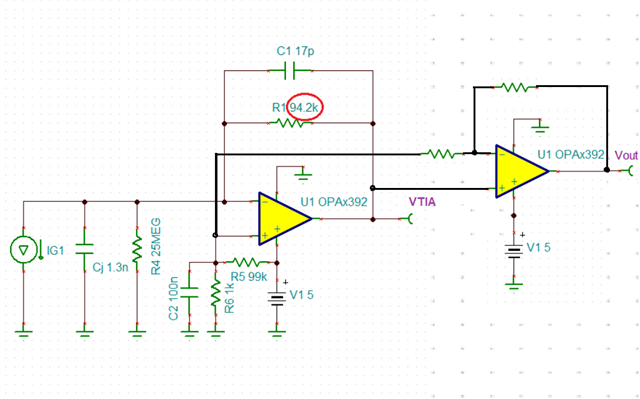
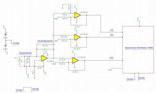
Initially the design used an OSD15-5T Photodiode. Now, I was thinking of using one with a bigger surface area so that more light is seen by the photodiode. After wiring up the circuit (with the bigger photodiode - OSD50-5T), I can see that the output voltage of the Transimpedance amplifier goes negative when I blank/darken the sensor and it hits the positive rail when I open it. Please note that the diode is connected with 0 bias voltage (Cathode facing the -ve input of the Opamp).

Can the photodiode current change polarity when it goes dark (my initial thought is NO)? 

Or

Can this be fixed by adding a bit of bias to the +ve terminal?

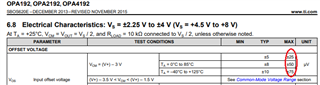
The TIA has bipolar rails (+/-5V). Because our system only uses the 0-5V range for the A/D converter, is it better to have the OPAMP connected to a single positive rail rather than Bipolar rails (+/-5) as it is currently?

Many thanks

Mathew

  • Mathew,

    The output of your transimpedance amplifier may go negative under dark current condition because of the negative offset voltage and/or IB current.  But then to hit the positive rail when you disconnect the photodiode, it would probably have to operate open-loop, have a large leakage current or to oscillate - to say anything more, we would need to know the magnitude of the negative voltage and see details of your circuit including op amp model and values of the components used. Keep in mind that no op amp output may swing all the way to its  rail so on a single supply, you will not be able to measure low current levels until the current is high enough to lift the output above the minimum voltage specified in the datasheet - see below.

  • Hi Marek, 
    Please see the circuit below for reference.


    The output of this TIA is followed by a voltage follower stage using the OPA292

    I did the AC analysis and can see that the output is quite flat with a nice -3dB point and no peaking. 

    would adding a little offset (approx. 200mv) be sufficient to stop the output of this stage from going negative and affecting the other circuits (as the MCU will only read 0-5V signals).

    thanks

  • In order to measure a dark current, you need to lift the OPA192 output 200mV above ground into its linear voltage range.  This will allow precision measurement of input current from 0 to ~48uA - see below.

    Assuming the impedance and junction capacitance of the photodiode is correct, the circuit is stable with 73 degrees phase margin - see below.

    However, if you need 5V single supply operation, you should probably use a low voltage op amps like OPA392.  This will allow higher performance and wider output voltage swing within 50mV to either rail - see below.

    The circuit is similarly very stable with 73 degrees phase margin.- see below.

    Attached please find the Tina-TI schematics. 

    Mathew's OPA192 Transimpedance DC sweep.TSC

    Mathew's OPA192 Transimpedance AC stability.TSC

  • Hi Marek,

    thanks for your reply. I don't need to measure dark current. What I need to do is to measure the photodiode current minus the dark current. this would mean that According to the datasheet, the maximum Dark Current generated by the device is 15nA (typically 5nA). So if we have 15nA going through the 95.3k feedback resistor, then the output voltage should be 1.43mV. 

    How would that be implemented in the circuit without the output going to negative? Would adding a bias help out?

    thanks

  • Mathew,

    No op amp output can swing all the way to its rails and thus the limitation of the output range has nothing to do with your dark current.  Conditions of the AOL define the linear range of the output voltage swing as it may be seen in the datasheet (see below) it is for OPA192 300mV away from rail for 10k load (~200mV for RF=100k) and around 50mV in case of OPA392. Thus, you should use the circuits just the way I showed you in my previous reply.  Allowing the output voltage any closer to negative rail will result in non-linearity and therefore erroneous measurement.

  • Hi Marek,

    Can you please explain why the inductor is  in the feedback loop in the second circuit? Is this modelling parasitic inductance?

    Many thanks 

    Mathew

  • Marek,

    I wanted to mention that in the existing design, the Transimpedance Amplifier is connected to a Voltage follower which is then connected to 6 amplifier stages - each with 4x gain the previous level for e.g. 1,4,16 etc.

    I have reworked the circuit as you mentioned, however, this time, I have added a Buffer and DiffAmp stage. The reason for this is because with the 50mV bias (on the Transimpedance Amplifier output), this voltage would be amplified by the subsequent amplifier stages (in the current design) and hence at low light levels, the ADC would always read Full scale voltage. The DiffAmp should "nullify" the 50mV offfset voltage and give some sensible readings at higher gain stages. 

    Please see the updated circuit below.

    Circuit with Buffer and Diffamp stage:


    DC Transfer Function of the above circuit showing DC Offset Nulling effect

    AC Transfer function

    From the DC Transfer function, it can be seen that the DiffAmp is doing its job of nulling the offset.

    From the AC Transfer function, there seems to be some peaking happening on Vout3. 

    I would like to know your thoughts on this?

    thanks

    Mathew

  • Mathew,

    In a real circuit the 1T inductor and 1T capacitor are NOT there - they are ONLY present for simulation of the open-loop gain (AOL) and inverse-beta (1/beta) curves for visual determination of the AC stability of the circuit.  Please review TI Precision Lab training material under following link:

    https://training.ti.com/ti-precision-labs-op-amps-stability-introduction?context=1139747-1139745-14685-1138805-13848

  • Mathew,

    I have previously level-shifted the output of the amplifiers to avoid non-linear operation in a single supply application because I thought you wanted to use only 5V single supply. But since I see that you continue to use +/-5V supply in the last stage, it makes little sense to level-shift the first two stages and then reference the signal back to ground using dual supplies.  In such case, the entire application may be implemented with a single stage OPA192 with far fewer errors coming from multiple offsets and gain errors - see below.

    8524.Mathew's OPA192 Transimpedance DC sweep.TSC

  • Hi Marek,

    Thanks very much for your response. This is how the circuit is connected right now. the +ve and -ve rails are +/-4.98V respectively. The Inverting Input is connected to GND and the Non Inverting input is connected to the Photodiode, however, this gives me a negative voltage (approx. -5mV) on the output as soon as I darken / reduce the light brightness to really low levels. As I mentioned before, the subsequent stages are 6 amplifier stages each with 4x gain of the previous stage. 

    Due to the fact that the output of the first stage is going negative, the rest of the circuit amplifies this and hence the output is saturated negative - which in turn is not read by an ADC with a range 0-5V. 
    I am not sure why the output of the 1st Stage Opamp is going negative. This means that any low level currents are not measured by the system and hence negates the use of a larger photodiode. Hence my reasoning for applying a bias to the Non-inverting input. 

    Please note that this issue was not visible when using a smaller Photodiode and there is no requirement to use bipolar supplies (provided the single supply solution can give a sensible result - which I believe may be difficult especially due to the AOL Voltage limit.)

    Hope this helps

  • Mathew,

    The circuit would not work the way you describe: "The Inverting Input is connected to GND and the Non Inverting input is connected to the Photodiode."

    A picture is worth thousand word - please use the attached Tina-TI schematic to make changes.

    5633.Mathew's OPA192 Transimpedance DC sweep.TSC

  • Hi Marek,

    Apologies. I described the circuit wrong. You are right. The circuit is connected as you have shown. The Non-inverting input is connected to GND and the inverting input is connected to Photodiode cathode (Photodiode Anode to Ground).

    Can you think of any reason why the output of the Transimpedance amplifier would be stuck at 5mV (even when running from bipolar supplies)? The simulation works fine, however, I am not seeing voltages close to the simulation results.

  • On a single supply under dark current conditions, OPA192 output would exactly be stuck at 5mV because this is the closest it can get to its negative rail - see below.

    However, I do not believe this to be true on dual supply - the output should only be at 5mV for 52.5nA photodiode current - see below.

  • Hi Marek,

    The Photodiode is mounted on a PCB with the Transimpedance Amplifier. The Photodiode has had multiple heating applied to it (when either taking it OFF or putting it back on). similarly, the Opamp is situated in very close proximity to the Photodiode that any heat applied to the Photodiode will be applied on the Opamp as well. Could there be a chance that the Photodiode or Opamp may have been damaged due to constant removal and fitting?

    I tried checking the output of another similar transimpedance amplifier with a similar photodiode and under low light conditions, the output doesn't seem to go under 0V. I didn't check the subsequent Gain stages to see if there was any voltage there or if the Opamp was just outputting 0V (My DMM only goes down to 3 significant digits). 

    Could the Photodiode or Opamp be doing something weird? 

    I shall try changing the Opamp and the Photodiode tomorrow  to see if the problem goes away.

    Any other suggestions are welcome.

  • Mathew,

    It is highly unlikely that under the dual supply conditions and dark current the output happens to go to 5mV but it is very likely that is what you would see under a single, 0/5V, supply. Heating OPA192 to 125C could increase the IB up to 5nA (see below) but this would result in Vout of around 0.5mV unless the temperature is raised to around 160deg C.

    Having said that, exposing OPA192 to temperature above the Absolute Maximum Rated temeperature of 150 deg C (see below) could permanently damage the part.  As far as the photodiode goes, you need to check its datasheet for its maximum rated temperature.

  • Hi Marek,

    After a few days of testing, I replaced the Opamp with an OPA380 (which is a Transimpedance amplifier) that allows upto 0V measurement. 
    the part seems to be better than the OPA192 with regards to signal output. 
    At low voltages, the Second Gain stage I mentioned before (Gain x1024) shows voltage of approximately 8mV. However, this seems to be fluctuating between the + and - milliVolt range. 

    what I did notice is that on the OPA192, the ambient temperature affects the signal (in the sense that it goes more -ve when the OPAMP is cooled).  the OPA380 is also affected, however seems to recover pretty quickly.

    All these tests are done in a Dark room with a Halogen Lamp running from DC to provide a clean signal. this room is air conditioned and hence is at a set temperature of approx. 20-22 degrees C. 

    At these low voltages, am I right in thinking that noise is messing up the signal. ? 

    I am attaching the OPA380 schematic here FYI.

    Many thanks

    Mathew

  • Mathew,

    The only reason OPA380 may swing all the way to 0V is that use you use 2k pull-down resistor to -5V supply, which diverts the output stage quiescent current from lower output transistor, thus turning it off - without it, OPA380 could only swing within 100mV above ground.  Adding 5k pull-down resistor to -5V will likewise allow output of OPA192 to get to 0V.

    There are two reasons for fluctuation of the output voltage:

    1. integrated noise - you should be able to filter it out with a low-pass filter at the output or much larger feedback cap (either one will limit the bandwidth)

    2. input offset voltage temperature drift

  • Hi Marek,

    Thanks very much for replying. 
    I could see that without the 2k pulldown resistor, the output voltage was reading approx. 45mV (although the spec says it should be more than 100mV). 

    Secondly, the voltage that I am seeing is measured before a low pass filter (8.2k & 47nF). This would create a -3dB point of 413 Hz) - which would limit the bandwidth. However, I am not measuring fast light changes. 

    Your second point about input offset voltage temperature drift is interesting and I would like to know more. Also if possible can you suggest a few ideas I could try reducing this? I suppose the obvious one would be to stabilise the temperature and maybe enclose the Photodiode and Transimpedance Amplifier in an enclosure?

    Any ideas are welcome. 

    Many thanks

    Mathew

  • You read 45mV of called slammed output swing where the outpout transistor operates in a non-linear region and is fully trioded against the rail while the datasheet shows a linear output swing of 100mV where op amp maintains high open-loop gain. 

    There is nothing you may do to change the offset temperature drift other than keep ambient temperature constant but with OPA380 maximum drift of 0.1uV/C I doubt you can do much better.  Of course, in the high gain of 1024, you may see output flactuation of +/-1mV but if the temperature is kept within ~2 deg C, it is most likely due to noise - that is why you need to measure the voltage after your low-pass filter to filter out the noise.

  • Hi Marek

    thanks for your reply. 
    To measure low light levels  from the OSD50-5T, I have now increased the gain to 4.7Meg. The feedback cap is 27pF. 
    The output of the buffer stage (after the transimpedance stage)  is now measuring up to -5mv. 
    is the only way to stop this from happening by applying a bias to the +ve input of the Transimpedance amplifier to 100mv and then nulling this later or would it be better to remove the 2k resistor?

    I think looking at the the data sheet, it mentions that the 2k resistor can be connected to Gnd. In that case the output will be limited to max 60mv (from Gnd)

    secondly any ideas on  what could be causing the noise  and any suggestions for clearing this ? 

    thanks

  • Are you using OPA380 or OPA192?  If the dark current is still 15nA, using TIA of 4.7M should lift the output to arounf 70mV so I'm missing some info here.  Please attached the Tina-TI circuit schematic with your latest modifications including your second stage - picture is worth thousand words...

  • Hi Marek,

    I am using OPA380 because it is a Transimpedance Amplifier compared to the Precision Opamp OPA192, and also because it allows a "true zero" output for no light. The dark current stated is still the same (15nA max). Please note that the supplies are reading +/-4.98V (Not 5V as shown in the schematic).

    I am attaching the circuit here FYI.

    TIA with x1024 Gain Stage.TSC

    Many thanks

    Mathew

  • Mathew,

    As I wrote before, most op amps (not just OPA380) may be driven to ground on single supply by using a pull-down resistor to a negative supply.

    Since max Vos of OPA380 and OPA192 is =/-25uV, for zero input current, with the overall gain of about about 1,000, the output may be anywhere between +/-25mV. You read 5mV at Vout3 only because the offset happens to be 5uV but another part may be up to +/-25uV.

    However, since you use the dual supplies in gain stages 2 and 3, why not to use OPA192 with dual supply also in the first stage. This will eliminate need for pulldown resistor. Additionally, I do not see a reason for second stage buffer - see below.

    All and all I would recommend you to use circuit shown below.  This will eliminate the need for one of the op amps as well as a pull-down resistor.

  • Hi Marek,

    Thanks very much for responding. I have a few ideas which I want to know if they would work. 

    I know that I mentioned that I was using the OPA380 instead of the OPA192. The PCB that I was working on was built to house the OPA192 and hence the OPA380 was connected using mod wires (rat's nest)and hence was not a good design for noise stability. 

    Therefore, I decided to go back to the OPA192 (hence the circuit is connected exactly as you mentioned  - with the exception that the Buffer stage is in the circuit path - which I am also thinking of removing in the next iteration) and am now thinking of the following ideas (Please see the schematic attached in this reply).

    your idea of the offset swinging between +/=25uV is very interesting and hence I am confident that this would explain why I am seeing varying amounts of voltage on the output of the TIA and Gain stage. 

    Idea 1: Monitor Vout3 (output of 1024 Gain Stage) and apply an offset voltage (On TIA) to make Vout3 +ve or close to 4mV. The reason for 4mV is that the gain stage is connected to a 10 bit ADC (running from 5V). This would mean that the lowest voltage the ADC would read is approx. 5mV (4.88mV). 

    Idea 2: Monitor Vout1(output of TIA) and apply an equal and opposite voltage to the Non-inverting input of the TIA to "zero" it while darkening/closing the Photodiode completely. This would mean that 0 light levels, the 1024 Gain stage would see a +ve voltage always 

    Does any of these sound like a viable option. Obviously, this is done in a Thermally stabilised environment. 

    OPA192 Ideas.TSC

    Or this one

    Many thanks

    Mathew

  • Are you saying the the variation in the output voltage you reported were for different op amps?  If so, obviously each op amp has different offset that follows normal Gaussian distribution that changes over temperature - see below.

    Let me start with your IDEA 2: even if you could null the output of Vout1 to zero, you could still have an error up to +/-25mV at Vout3 due to Vos2 up to +/-25uV - see below.

    Thus, the only way to null the offset is to look at Vout3 and adjust the Vnull BUT I do not think you may  have means of adjusting it to required uV level so you get 4mV at Vout3.

  • Hi Marek,

    So, what is the best way I can achieve this? 

    Do I need to use a zero drift OPAMP ? 

    What would be the correct way forward?  I did initially think about how I am able to generate a uV level signal as the bias voltage. 

    Many thanks for your help.

    Looking forward to a reply,

    Mathew

  • I think the best way to do this is by calibrating the system and make all necessary adjustments in software. 

  • Hi Marek,

    So am I right in thinking that if I put a bias voltage of let's say 10mV (for a Transimpedance circuit hat runs on dual supplies), then I suppose are you suggesting that this 10mV signal is deducted from the ADC Reading (in the software) 

    Or

    Connect this 10mV signal to the ADC -Vref instead of Ground reference (Hence raising the ADC 10mV from GND)?
    If so, then do the other gain Opamps need to be biased to this 10mV signal?

    thanks

    Mathew

  • Mathew,

    Could you please tell me what is the range (min/max) of the current you try to measure.  Also, do you prefer single or dual supply?  If you can calibrate the system in software, your application can be easily implemented (without feeding any precision voltage) by offsetting the output in hardware in order to stay in linear output range of the op amp and input range of ADS you use make the measurement.  Btw, what is the input voltage range of the ADS you use?

  • Hi Marek,

    The current range is between 0-52uA. 

    the current circuit is using a dual supply. I am not sure why one would use a dual supply instead of a single supply. Is it to keep the linearity of the system? Or is it to maximise the dynamic range of the sensor? 

    Currently, I have no access to the software and hence the "fix" needs to be done in hardware. I did not design the existing hardware. This was done by someone else.

    For the time being, I have found a suitable work around for this issue. I found out that applying a small bias voltage at the non-inverting side of the Transimpedance Amplifier will make the highest gain range (1024) output read approx. 5-15mV which equates to roughly 1-4 ADC bits (at dark). this will make sure that the output does not go below the 0V and hence the ADC would read all positive voltages.

    The input voltage range of the ADC is 0-5V (approx. 4.99V ). 

    Thanks

    Mathew

  • Mathew,

    We make a full circle here.  Below please find the trans-impedance amplifier solution that would stay within the linear output range of OPA392 (0.05V to 4.95V) for 0 to 52uA photodiode current.  If you need precision, you should calibrate the circuit for IG1=0 and IG1=52uA by measuring Vout and using it to determine initial error (away from 50mV) and actual gain (due to tolerances of the resistors) by accounting for their value in your post processing of your ADS readings.

    It take 17pF feedback capacitor to assure AC stability of the configuration - see below 63 degrees phase margin.

  • Hi Marek,

    the above solution looks good and can be implemented in the next iteration of the system PCB. 

    The main issue I am having right now is that the existing Analog Front End of the system is not performing according to my needs. I am seeing that the measurements drop a lot earlier than usual (at low light levels, the 1024 gain range is being used, however upon closer inspection of the output voltages of the other gain stages, I can see that the output starts to go negative from the x16 gain range and by the time I measure the 1024 gain range, the output is at -250mV approx).

    Please note that currently, the 6 Gain stage are divided as follows (Transimpedance stage uses OPA192, x1(buffer) & X4 uses OPA2192, X16 - X1024 uses OPA4192).

    The solution that you mentioned looks like it would certainly work, however, for the time being, I only have access to the hardware side and not the software side. Your suggestion can be implemented in the next iteration of the whole PCB as then I would have full control over the Hardware and software. 

    As I mentioned before, the initial circuit was designed around the LTC1053 Opamp, but this is now obsolete. Then we moved onto the OPA192 which seemed to be better than the LTC1053 and we did see mixed improvements, however, now we are at the stage where we want to use the system to its full extent. However as I mentioned, this threw a  spanner in the works and I am trying to fix this. Most of these issues were present in the old design as well.

    One work around was to apply a very tiny (< 5uV) signal onto the Non-inverting side of the Transimpedance Amplifier thereby setting a dark light level which would translate to 0 bits for a 10 bit ADC (<=5mV). Currently I am using a 10Meg resistor and 470 Ohm resistor to drop the 5V supply and then through a POT, adjust the voltage till the 1024 range reads approx. 5mV @ dark.

    The photodiode is connected as zero bias mode therefore, the dark current should be 0. 

    I know that applying a bias voltage to the non-inverting side would reverse bias the Photodiode and cause it to generate dark current, but as long as the output voltage (1024 gain range) is staying at or around the 4mV level, then the ADC would read 0. Is this right?

    an alternative method would be to use a 12 or 16 bit DAC to generate a lower voltage (from 5V) and then divide it down and then through a POT to generate an adjustable voltage reference. 

    I know that this forum is only for Texas instrument devices, however, I just thought to put this as well. I have found another Opamp from LT (LTC2054) which has better Offset qualities than the OPA192. 

    the next iteration Analog board would be using this on all the Gain stages (including the Transimpedance Stage) wired for Dual supply. What do you think about this?

    thanks

    Mathew

  • It would really help if you attached your schematic.

  • 5710.OPA192 Ideas.TSC

    Hi Marek,

    I am attaching the TINA file FYI. I have only put the 1024 Gain range circuit and not the others. If you want me to re-do this with the other gain stages, then please let me know.

    Thanks,

    Mathew

  • Mathew,

    Your circuit has too much gain so the second stage, Vout, already saturates against the rail at 175nA - see below - and therefore is unnecessary.

    Since you operate on dual supply, you need to be able to adjust the pot in either direction to null up to +/-25uV offset of OPA192 all the way to zero.  For this, you should use two 10M resistor with 200ohm pot that will give you +/-50uV adjustment range - see below.  Btw, f you supplies are significantly varying from +/-5V, you may need to use larger pot resistance to get the required range.

    Running AC stability with 10pF feedback cap, results in 91 degrees phase margin - see below.

    Running transient analysis confirms stable operation with 10% small-signal overshoot - see below.

    I have attached below Tina-TI schematics for your convenience.

    OPA192 transimpedance_ML.TSC

    OPA192 transimpedance AC stability_ML.TSC

  • Hi Marek

    Thanks for your reply. 
    the reason for the high gain on the second stage is to measure low light levels (<100 lux).

    the system does not measure fast changing signals. The bandwidth requirements are not that stringent ( probably less than 10k. )

    is there anyway to fix this offset voltage using fixed value resistors rather than a pot? My main concern using a pot is that the application is used in very harsh conditions where there is quite a lot of vibration . 

    would this offset voltage explain why I am seeing the output voltages on the gain stages go negative ? 

    in the above picture I can see that you have put a 1k into the signal path . Why is this there ? 

    thanks

    Mathew 

  • In order to completely eliminate the error related to +/-25uV offset of OPA192, you would have to either:

    1. calibrate it out in software

    2. adjust in hardware (pot)

    3. ignore it

    Since the offset voltage can be either positive or negative, under no current (dark current) the output could go 25uV or more negative (see below).

    To the last point of ignoring the offset by grounding the non-inverting input - even if you assume that the max offset at 125C to be +/-75uV, the max current measurement error this could cause is +/-0.8nA (+/-75uV/92.3k).

    I did not have 1k in the signal path in my original schematic - I kept it only because you showed it in your attached schematic - I thought it might be there for overvoltage protection.  If that's is not the case, remove it as it does nothing for measurerent. 

  • Hi Marek,

    thanks for your support. 

    what I have found is that cleaning the PCB thoroughly (giving it some PROPER TLC - IPA Wash, Clean with anti static brush, compressed air , hot air drying and leaving it to cool to room temperature), made the circuit work ( previously, this test PCB was not working and hence the other gain stages were going negative). I also noticed that temperature also plays a big part in the design. In the final product, this PCB is enclosed in a box that is temperature controlled. Therefore, all readings are taken in a constant temperature. 

    for the time  being, the circuit would have to be kept as it is and cleaned thoroughly. Later on when I do re-design the board, I'll be looking at your circuit suggestion and implement that. 

    I am going to clean all the PCBs using ultrasonic cleaner and then test them. If this works, then we have a very good solution if not, then its back to the drawing board Disappointed and more hair pulling and I'll be back onto this forum.

    Many thanks for all your help Marek,

    Much appreciated.

    Mathew

  • Hi Marek,

    Just wanted to ask something trivial. If I was to use this circuit as you showed, how would I connect the other Gain stages to the Transimpedance Amplifier output? Would they need to be biased to the same bias voltage as the TIA? and would this bias voltage be fed to the ADC so that the ADC can deduct this voltage from the ADC reading? 

    If  so,  how would the ADC be referenced? would it be referenced to GND or the bias voltage? hope this makes sense

    Many thanks

    Mathew

  • Hi Mathew,

    Sorry for the delay on this one. Marek is out of office. I will work with him when he gets back to get an answer over to you. 

  • In case of OPA192 using a dual +/-5V supplies (with VTIA nulled to zero), you would simply connect VTIA to the input of second stage as shown below.  The ADC input would then be reference to GND.

    In case of OPA392 using a single 5V supply, you would feed the VTIA output directly into the non-inverting input of the second stage while referencing the output to 50mV as shown below.  Then ADC would also need to be referenced to 50mV by subtracting it in software from actual ADC reading.

  • Hi Marek,

    thanks very much for your valuable input. I think I have grasped the idea. 

    Please see the circuit below. the resistor and capacitor values are not correct, and it is missing some other circuitry. However, this is just a sketch of what the solution would look like.

    I believe  this would work with 12 or 16 bit ADCs as well, as the reference voltage can be nulled out in software (as you mentioned).

    The Photodiode is connected as a differential mode to prevent the reference voltage from impinging a reverse voltage across the photodiode and hence reducing dark current to almost 0.

    I presume the ADC REF GND would be connected to the Analog ground ? - which in turn is connected to the digital GND somewhere else.

    Many thanks,

    Mathew