This thread has been locked.

If you have a related question, please click the "Ask a related question" button in the top right corner. The newly created question will be automatically linked to this question.

XTR110: How to use 200mA on page 9 of the datasheet.

Part Number: XTR110

Hi ,

I want to use XTR110 +/-200mA AO circuit, but it doesn't work.

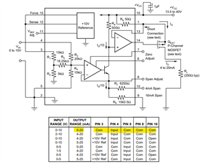
It was designed as shown in the Datasheet Page 9.

I couldn't find IR9513, IR513, and IRFF9113, so I used RD3L01BATTL1 , FDD86381-F085, and RD3L140SPTL1 as substitutes.

Please check my circuit.

  • Hello,

    What is the size of the load you are trying to drive? When you say it "doesn't work" do you mean you can't get the full scale current range (all the way up to +/-200mA) or something else?

    Cheers,

    Jon

  • Hi ByungJin,

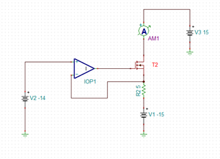
    Unfortunately it appears the circuit in the data sheet is drawn incorrectly; the NMOS, T2, is the wrong orientation.  The way it is drawn, the source is connected to the output, with the drain on resistor R2.  As it is, this leads to the NMOS body diode connected from the output to R2. This is incorrect.

    The image below shows the correct orientation.  In the schematic below (set up with comparable voltages from the circuit), AM1 measures 200 mA, which is the correct current value.  The NMOS T2 should always be sinking 200 mA, the PMOS T1 will supply current from 0 mA to 400 mA, which leads to an output current swing of -200 mA to +200 mA.

    Can you reverse the drain and source connections, and try again?

    Best Regards,

    Mike

  • When tested as informed, T1(Q1) or T2(Q3) FET generates a lot of heat.
    What's the problem?

  • Hi ByungJin,

    I would expect the FETs to get hot, there is a significant amount of power dissipated in this solution.  T2 will always sink ~200 mA when working properly, and, the current through T1 will be 0 to 400 mA depending on the signal amplitude.  At the peak output current, 400 mA will be conducted through T1, and, if the IO node is referenced to ground, this means 15V*0.4A = 6 W will be consumed on T1 alone, and 15V*0.2A = 3 W on T2.

    You should certainly pay attention to the thermal dissipation on T1 and T2. Be sure to follow best thermal layout practices and have good thermal conductivity from the device to the board or to a heat sink to minimize the die temperature on these FETs.

    Best Regards,

    Mike

  • Thank you.

    Then, how can I modify it to +/-10mA circuit?

  • Hi ByungJin,

    The first step is to lower the sinking current that flows through T2 and R2 from 200 mA to 10 mA.  This can be done by increasing R2 to 100 Ohms.

    The second step is to change the current that flows through T1 from 0 to 400 mA to 0 to 20 mA.  You have a couple of options here.  The first option is easiest, given that you already have figure 8 connected-  that would be to change the resistance of R1 from 2 Ohms to 40.2 Ohms. (20x larger).

    The second option would allow you to use the internal resistors on XTR110, but you would need to change the configuration.  The XTR110 allows for a 0 to 20 mA setting without needing the additional sense resistor, as seen in figure 1:

    In order to do this, you would need to change the sense connection from R1 (in figure 8)  to pin 1; so, you would remove R1, and, connect the source of T1 to Pin 1.  Then pins 9 and 10 would be connected to GND (same as Com, in the table).  Also, pin 3 would need to be connected to pins 15 and 12.  

    The advantage to the second option would be improved accuracy, since the resistor used is internal to XTR110, and the ratio between this resistor and the other resistors internal to XTR110 will be matched.

    Regards,

    Mike


  • Hello Mike,

    Please check one more.

    If i want to make +/-20mA circuit, must change some resistance.

    R2 -> 50Ohms, R1 -> 20Ohms

    Rights?

  • Hi ByungJin,

    Yes, that's correct- let me know if you have any problems with these configurations.

    Regards,

    Mike