Because of the holidays, TI E2E™ design support forum responses will be delayed from Dec. 25 through Jan. 2. Thank you for your patience.

This thread has been locked.

If you have a related question, please click the "Ask a related question" button in the top right corner. The newly created question will be automatically linked to this question.

LPV812: Offset matching

Part Number: LPV812
Other Parts Discussed in Thread: LPV821, LPV811, TLV2333, LM358, OPA627

I happen to have a design where the same input voltage is amplified with an inverting and a non-inverting amplifier (with similar gain actually).

The offset voltage of the LPV811/2 is naturally much bigger than from a zero-drift amplifier such as the LPV821.

In my case the parasitics would cancel out if there were a matching of the offset between the two channels.

The datasheet documents the offset distribution for channel A and channel B, pretty similar as needs to be.

But it does not state that the offsets (or bias currents) would be correlated, which I would expect they are due to symmetry (same die, same temperature, same supply, same common mode ...).

To which extent can it be expected that the non-idealities are "matched"?

Is an estimate of a factor 10 reasonable (i.e. 10% do not cancel out)?

Would a similar argument apply to say the TLV2333?

Are there OPAMPS for which such a correlation is specified (I didn't look everywhere)?

  • The two input transistors of a single opamp are placed near each other on the die so that they have as much the same characteristics as possible. This implies that any differences are caused by local changes on the die.

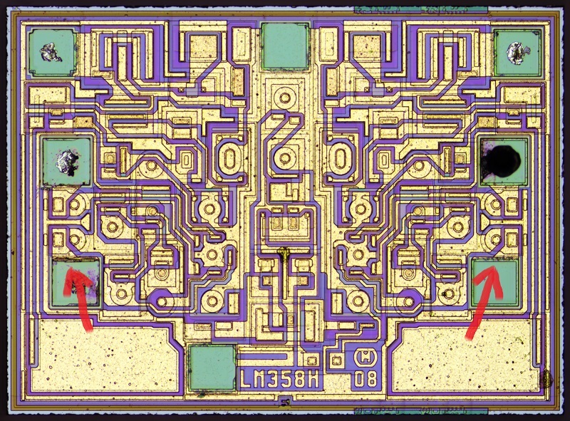
    The input transistors must be near the input pins, so the inputs of different opamps are usually far apart. See, for example, the LM358:


    (source: zeptobars.com/en/read/TI-LM358-dual-general-purpose-opamp)

    This means that the input offsets of the two opamps on the same die are pretty much independent of each other.


    For an opamp with resistor trimming or e-trim, the remaining offset depends on the accuracy of the trimming mechanism, which is independent of the die. The same principle applies to chopper opamps.

  • Tnx, I understand the point.

    I am not a low-level chip designer, so I do not know what the root causes of e.g. an offset are.

    I was assuming that process variations may cause it.

    Practically thinking a misalignment of masks in the manufacturing process may cause it.

    But then though local, the effect on the second OPAMP on the other end of the chip may still be correlated - same mask misalignment (even with a stepper).

    How local are the effects that cause an offset?

    I have difficulty to imagine such narrow causes.

    On the other hand I can imagine contributions to offset that are correlated across the die e.g. temperature.

    Anyway: The argument is clear, is it also empirically verified i.e. measured?

    Is there really no significant correlation?

    In another thread I read that variation (of e.g. AOL) can go down to 1% across the same wafer. 

    It surprises me that offset should be THAT local.

  • Mask misalignment would affect both transistors in nearly the same way, so it would not generate much of an offset.

    As far as I know, local variations are caused by impurities in the silicon, and variations in the chemicals used when etching. The differences are smaller in nearby areas.

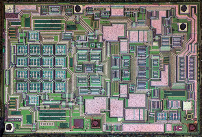
    Placing the two input transistors near each other is so important that some opamps use multiple transistors in parallel for each input and interleave them, so that local variations affect a similar number of transistors of each input. For example, the OPA627 has eight transistors per input, in a 4x4 pattern:


    (source: www.richis-lab.de/Opamp22.htm)

  • As Clemens said, there is absolutely no correlation between offsets or IB's (in CMOS) of two channels on the same chip because ALL variations on a good layout are caused by wafer fab process under and/or over-etching of diffusions.  This is, however, not the case with misalignment of masks because then the offsets of both channels would be shifted in one direction (a systematic error) and result in both channels having "matching" away from zero. In general, all specs centered around zero have no correlation because the only reason for them not being zero are controlled by the physical limitation (resolution) of the lithographic process used to manufacture ICs.  For this reason they are random in nature and thus follow Normal Gaussian distribution centered around zero.

    Having said that, in case of bipolar input transistor op amps with no IB cancellation, IB's of both inputs (or channels) flow into input terminals for npn and out for pnp - in such case there is matching within 10% (bipolar transistor variation of beta) because IB's in such case are not centered around zero.

  • I like to learn and asking makes us learn.

    It's a pity that I cannot exploit a correlation, but at least now I know why that is.