This thread has been locked.

If you have a related question, please click the "Ask a related question" button in the top right corner. The newly created question will be automatically linked to this question.

THS3062: Question about the Power Pad on DDA Package (SOIC-8-PP)

Part Number: THS3062
Other Parts Discussed in Thread: LM7372, LM2679, LM2673

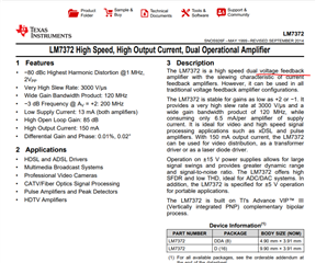
On one of the circuits that I built, I used the LM7372MRX Op-Amp, a dual, high-speed op-amp in the 8-pin DDA package. According to the datasheet on section 5 page 3 under Pin Configuration and Functions, the exposed pad should be tied to ether V- or left electrically floating. Since they said that the die attach material is conductive and internally tied to V-, I connected it to V- on my PCB.

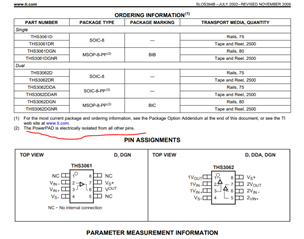
Now, as a test, I want to try and use a different op-amp. As the title suggests, I want to try and use the THS3062 DDA package. My concern is with the exposed pad on the THS3062. According to the datasheet on page 3, the PowerPAD is electrically isolated from all other pins.  Considering how it is electrically isolated from other pins, would it be safe to solder the THS3062's PowerPAD onto a pad that is tied to V- on my PCB? Will it harm anything in my design? I am only doing this as a test so I would like to try and not have to make a new PCB just to test this op-amp. 

If it helps, my power supply is +10 volts and -10 volts. The THS3062 will run off of this split supply, and we're only driving small-signals at 100 mV peak to peak. This isn't used for any high-power devices.

  • Morning Jason, 

    The THS3062 is a on a very old Bicom1 process that is in fact dielectrically isolated substrate material - hence, you can indeed connect to a heat spreading plane tied to the negative supply - I would current limit those supplies initially on turn on just to be sure, but it should be ok, 

  • You do know you are going from a voltage feedback op amp to a current feedback one - be careful to have the Feedback R in the right range for THS3062 stability. The LM7372 is in a class of high transconductance VFA which would have higher input voltage noise to get that slew rate. 

  • Thanks for your reply. I think I understand the implications of switching topologies. I'm doing this on a new, clean board,  and I'll use recommended resistor values as shown in the datasheet (560 ohms) for a gain of -2 or -1 (inverting sum/difference op-amp configuration).I thought that it was VFAs that were supposed to have better input voltage noise compared to CFAs.

    You mentioned current limiting the supplies. How much current do they typically draw on startup? I'm running this at +10/-10 volts,but I can always reduce it to +5/-5. That would be unfortunate if my supply can't handle it. Theoretically, my supply can handle 3 amps (coming from a supply based on the LM2679 and LM2673).

    If I may add on, while it may be not ideal, what if I used an SOIC package instead to ignore the PowerPad? Certainly thermal performance would be worse, but this is just prototyping to see if CFAs would be a good fit, not for commercial use.

  • Different kinds of VFAs can have lower noise, but this very high slew rate input stage is higher than CFA usually - if you look at the specs, that is clear. 

    I only meant initial turn on current limit to be safe for validation, then let the supply run with a current limit adequate to the signal requirements. 

    You could also use the PPAD package with no pad under it if you continue to be concerned. That came up a lot for people replacing standard SOIC with PPAD packages in existing layouts.