Because of the holidays, TI E2E™ design support forum responses will be delayed from Dec. 25 through Jan. 2. Thank you for your patience.

This thread has been locked.

If you have a related question, please click the "Ask a related question" button in the top right corner. The newly created question will be automatically linked to this question.

LMH6321: Best Circuit to use LMH6321 to high parastic capacitive (500p) load and high frequency (20Mhz)

Part Number: LMH6321
Other Parts Discussed in Thread: TINA-TI

Hi Team,

Good day. I have a high-speed signal coming to a PCB and I wasn't able to use the high-speed signal (about 20Mhz) directly to the digital input-output card, because of high parsatics capacitance (about 400pf probably). So now that I use LMH6321 as a buffer to improve the slew rate. Please find the schematic for the same.

I see some delay than expected in the real PCB.

I left the CL open. ( would it cause a problem?)

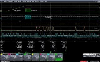
also attached are some scope signals for 5Mhz as input and 20Mhz as input.

green signal- output from the buffer LMH6321 and Red signal- input to the buffer.

So my questions:

1) I see that if we use some polarised high capacitors as supply bias pass capacitors, would it help to improve slew rate?

2) And is there some better circuit to use it as a buffer for high frequency(20Mhz) and high capacitive load(400p).

P.S I could also control my input at DIO to HIgh impedance or 50 ohms, if then what circuit can be best used?

Best Regards,

Tarun Kumar

Lmh6321.TSC

  • Hi Tarun,

    400pF means an impedance of 20 Ohm at 20MHz and 2 Ohm at 200MHz, if your signal contains harmonics. And a slew rate of 1800V/µs means output current spike of

    I = 400pF x 1800V/µs = 0.72A

    But the output short circuit current limitation of LMH6321 sets in at 300mA.

    Such a high current spike would be rather inappropriate for every circuit and would produce lots of EMI and ground bounce. Is there a chance to remove or at least decrease this 400pF capacitance? Where does it come from?

    Kai

  • Update:

    I have used a closed-loop config. And the driving capabilities look promising. What do you think? But the current through output shows a bit unrealistic currents. it's a good way to use it. 

    Lmh6321_closedLoop.TSC

  • Hi Tarun,

    where do the 400pF come from?

    Kai

  • Hi Kai,

    The parasitics come mainly at the input of a high-speed digital input-output module from NI (PXI 6555 module). 400pf is just a guess as i don't have any document stating it and also could calculate it at the moment. And other parasitics from some relays in the path( which are needed).

    Tarun

  • Hi, 

    You are right, for some time the circuit worked normally. But at times IC gets really hot and saw huge oscillation on the output of the buffer and also some other signals which are not related to the buffer

  • Can you give a link to the datasheet of this modul?

    I cannot believe that there's a 400pF at the input of a "high-speed" modul. In any case when you drive the board with an amplifier you should either isolate the output of amplifier from the cable impedance by the help of an isolation resistor or you should use series termination with the cable impedance. Would be interesting to see wether this high-speed modul has a 50 Ohm input.

    Kai

  • PXIe-6555-Specifications.pdf

    please find it in the attachment. 

    Would be interesting to see wether this high-speed modul has a 50 Ohm input.

    Yes,I can set the input to 50-ohm input or high impedance input.

    In any case when you drive the board with an amplifier you should either isolate the output of amplifier from the cable impedance by the help of an isolation resistor or you should use series termination with the cable impedance

    a small series Resistor of 1ohm should do?

  • Hi,

    I have attached some scope signals. and I see that as frequency increases, the output voltage is reduced.Is there a way to surpass that?

    Here attached 14 Mhz and 20 Mhz scope signals, are input to the buffer circuit attached here.

    Is there a better way to work this out? Thanks.


    Lmh6321_Working_HF_VD.TSC

  • Hi Tarun,

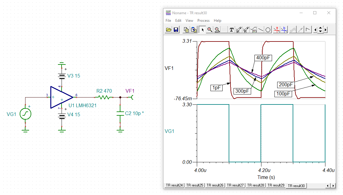
    first, I would try to confirm that the stray capacitance at the output of LMH6321 is really that high. You can check it with this circuit:

    tarun_lmh6321.TSC

    Mount the 470R resistor close to the output of LMH6321. Use a rather low signal frequency (here 5MHz) and compare the scope plot with the TINA-TI simulation. This should allow you to estimate the load capacitance seen by the output of LMH6321.

    Please post your scope plot here.

    By the way, do you use any cable at the output of LMH6321? If yes, how long is the cable?

    Kai

  • Hi Kai,

    Please find the scope find plots in the attachments. For all the above tests and this test, I used a jumper wire of less than 10cm.

    Red signal - input  and green - signal output

      ---> When i use High Impedance termination at the input of the digital card.

    (looks like the stray cap is around 200p.

     -->when i used 50ohm termination at the input of the digital card.

  • Hi Tarun,

    I have used a closed-loop config. And the driving capabilities look promising. What do you think? But the current through output shows a bit unrealistic currents. it's a good way to use it.

    Not the LMH6321 is driving the load but VG1 Relaxed

    Kai

  • oh yeah Sweat smile.  Any pointer to solve this ?

  • Hi Tarun,

    For all the above tests and this test, I used a jumper wire of less than 10cm.

    Oops!!! A single wire is no good idea in that frequency range. A single wire has some considerable inductance, about 1nH/mm as a rule of thumb. This would explain the ringing that can be seen in your scope plots:

    tarun_lmh6321_1.TSC

    Please avoid longer single wires at all. Use shortest wires. Every centimeter, yes, even every millimeter counts. Or better use 50 Ohm technique by having 50 Ohm termination resistors and a 50 Ohm cable, when longer distances have to be handled.

    Kai

  • Hello Tarun,

    Please keep us updated with your debugging and lab progress.  If I am understanding correctly, you are working on an actual PCB in the lab, as well as investigating simulations.  Please help me understand if that is not the case.

    Kai's points on proper termination and high speed layout are accurate; there is a lot to consider when undergoing high speed designs.  I would encourage you to peruse popular resources if you have a need to familiarize yourself with a curiosity or issue of high speed design.  And we are also here to help you Slight smile.

    Best,

    Alec

  • Hi Kai and Alec,

    Every centimeter, yes, even every millimeter counts.

    you were right. I have changed these wires to an enameled copper and I already see quite a difference.

     --> after changing to copper wiring at a clock speed 20Mhz

     --->befor coper wire at a clock speed of 17Mhz

    better use 50 Ohm technique by having 50 Ohm termination resistors and a 50 Ohm cable,

     yes, we will use it when we design our final PCB.

    Please help me understand if that is not the case.

    Yes, you are right , I am doing them simultaneously.

    I would encourage you to peruse popular resources if you have a need to familiarize yourself with a curiosity or issue of high speed design. 

    It would be great to if you share thoese.

    And one more question regarding the attached scope image

    basically now IC is producing a 20Mhz signal - which is the red signal, this signal goes into the buffer and comes out as a green signal

    My question is,

    In the signals in blue box 1, I see a shift in the signal but which is expected, but the voltage levels are alright.

    In the signals in blue box 2, I see a shift, as well as the voltage levels, are reduced...what do you think is the problem here?

    Also, I have attached here there the scope plot of  15Mhz, 16.6 Mhz, 17Mhz, 18 Mhz and 20Mhz, where I see this voltage decreasing trend as frequency is increasing

     -->15Mhz

     --> 16.6Mhz

     --> 17Mhx

     -->18Mhz

     --20Mhz


    Could you guys help me with this?

    Thanks.

    B.R,

    Tarun

  • UPDATE::

    Also, I have attached here there the scope plot of  15Mhz, 16.6 Mhz, 17Mhz, 18 Mhz and 20Mhz, where I see this voltage decreasing trend as frequency is increasing

    Now I have added another scope channel (yellow), which is directly measuring at the output of the Lmh6321

    A small copper wire of length 3 cm connected  in this fashion is connected between the output of Lmh6321 and the Input of the digital card

    Green signal - measured at the Digital card 

    What do you think is the problem?

    B.R,

    Tarun

  • Hi Tarun,

    such a copper wire is totally unsuited to tansport a 20MHz square wave signal. The inductance is way too high. I said "every millimeter counts" and you show a copper wire reaching from the earth to the moon Relaxed

    Another issue is the ground connection between the two circuits. Even if you decrease the length of this wire to zero, then you still have the inductance of the ground wire again ruining the signal.

    The issue of this wire is not only its length and inductance, but that it also forms a loop with the ground wire. You have to route not only the signal wire from circuit to circuit but also the ground wire close by. That is the main mistake here.

    You will need a solid ground plane with both circuits sitting on it. The distance must be the smallest technical possible, unless you use a terminated microstrip line. And the signal copper track must be as short as possible, best running directly over the solid ground plane.

    The scope plots show that you have unwantedly created a so called "delay line". This is what happens when you combine an inductance with a capacitance: A phase lag is produced delaying your signal. Also, high pass filtering takes place and gain peaking at the resonance frequency of LC series circuit. This together makes that your signal gets rounded and delayed and that pulses of certain lengths can even have an increased amplitude compared to the input signal. All this can be seen in the scope plots and tell the experienced designer that your setup is not suited to handle high frequencies.

    Kai 

  • Hi,

    Thanks for your clear explanation. Understood. Yeah, I had designed some circuit blocks in a PCB which will later be implemented in a high-density PCB. But during the testing process, we found that we need some buffer like LMh6321. so I used a Bus PCB and long ground Paths to characterize it, as shown in the attached pic. super messy.


    any suggestions or some nice resources to design PCB for these frequencies?

    B.R,

    Tarun

  • The issue of this wire is not only its length and inductance, but that it also forms a loop with the ground wire. You have to route not only the signal wire from circuit to circuit but also the ground wire close by. That is the main mistake here.

    could we produce this error using simulation for a better understanding of the decrease of the voltage?

  • Hi kai,

    i have improved a bit of the grounding and i already see quite a difference.

     --> 20Mhz clock frequency

     ---> 20Mhz input frequency.

    Thanks, kai.

    suggestions or some nice resources to design PCB for these frequencies?

    Some resources should be great

  • Thank you for the support Kai! 

    Hello Tarun,

       Here are some resources for PCB layout considerations for high speed design: 

       Another efficient method would be to use our device EVMs as a guideline which can be found under the Hardware development tab. We provide the Gerber files and guidelines/pictures in the product folder of the EVM and user guides. For example: www.ti.com/.../LMH6321MR-EVAL

    Thank you,

    Sima 

  • Thanks kai and Sima for you support