This thread has been locked.

If you have a related question, please click the "Ask a related question" button in the top right corner. The newly created question will be automatically linked to this question.

TLV9004: Unstable output of TLV9004

Part Number: TLV9004
Other Parts Discussed in Thread: LM3489, LP5907

Hello

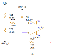
I observe a strange output of TLV9004. In the following schematic, the output of the amplifier should be roughly 1V, a DC value.

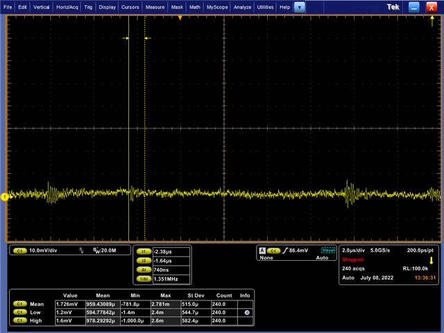
But I see a strange oscillation in the output. The output of the amplifier is connected to 1G3157 as one of the input. But when I remove the switch, the problem still exist.

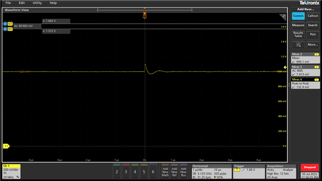
The non-invert input of the amplifier seems quite normal. But the invert input of the amplifier seem quite strange with the glitch.

Thanks for supporting

  • When does this happen?

    Are you using a switching power supply? Can you show the V+ waveform?

  • A LDO is used after the SMPS. I will capture the waveform tomorrow.

    Thanks for your fast response.

  • Hello, 

    Could you also clarify what V+ and V- values are? 

    Best regards,
    Ashley

  • V+ is 3.3V

    V- is 0V

  • Hi,

    this looks like a grounding issue. The signal ground doesn't seem to be clean and noisefree but seems to be contaminated by the SMPS switching noise. Keep in mind that LDOs have usually a very limited ripple rejection at high frequencies and because of this the switching noise can punch through the LDO and appear at the output of LDO.

    This means that the OPAmp sees a noisy supply voltage. But also the signal ground can be contaminated by this noise, because every supply voltage decoupling cap will shunt the HF content of switching noise directly to signal ground. And by flowing back to the source of switching noise -the SMPS- all the signal ground gets contaminated by this noise. As consequence ground is no longer ground, but it depends on where you measure the ground relative to the SMPS.

    The noise on signal ground can be injected into the input of OPAmp and by this appear on the output, or better said what the OPAmps makes with this noise. Or, if you connect the ground pin of scope probe to a distanced ground point, distanced to the ground pin of OPAmp, then you may merely see the ground noise dropping between these two ground points. In this case you may see noise, even if the OPAmp does not show any noise. The scope just shows the sum of two voltages then, the output voltage of OPAmp plus the ground noise. Because of this you should always connect the ground pin of scope probe with the ground pin of OPAmp when measuring the output voltage of OPAmp.

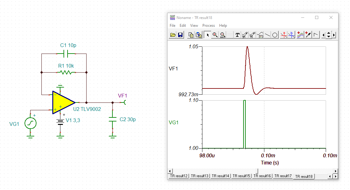
    When the noise is injected into the OPAmp via the inputs or the supply voltage pins then the output voltage will usually show a ringing with undershots and overshots, but without necessarily showing steep edges. The ringing is the consequence of R29, C10 and a bit load capacitance:

    user_tlv9002.TSC

    The edges are slew rate limited by the OPAmp and cannot be infinitely steep.

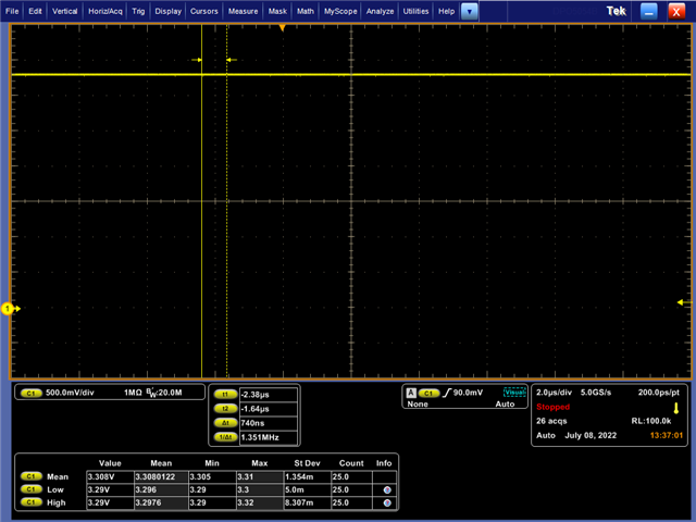
    But when the noise is coupled into the output of OPAmp, on the other hand, the output voltage of OPAmp looks a bit differently. Then the first edge of ringing is as steep as the noise pulse. The output of OPAmp is forced to follow this edge then because of the finite bandwidth and output impedance of OPAmp:

    In reality you will always see a mix of all these contributions, a bit from this and a bit from that.

    How to prevent all this?

    1. Install a low pass filter (Pi-filter) at the output of SMPS and feed the supply voltage including ground from this Pi-filter to the LDO, but not from the SMPS itself. Then the noise can no longer punch through the LDO and contaminate signal ground.

    2. Use a proper signal ground, best a solid ground plane to force that the ground is ground at all places on the board.

    3. To allow proper measurements with the scope use such a ground spring:

    Kai

  • Hello

    I use a LM3489 to create a 3.8V voltage, then use LP5907 to generate a 3.3V. It seems the ripple level of LP5907 is good.

  • Hi,

    the switching noise is not huge, but big enough to cause issues.

    How to proceed, depends on your application. If you can tolerate this noise, ok. But if not, then you should do something against it.

    Kai

  • Hello Kai

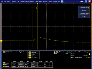
    I have some interesting founding that the glitch really link to the ADC sampling, the glitch happens when the ADC do the sampling. When I stop sampling, the glitch do not exist. Here is the detail of the glitch. it seems the slew rate is 0.1V/0.026us=3.8V/us, similar as the datasheet 2V/us.

    Thanks!

  • Hi,

    yes, an ADC input can also cause such a glitch. You didn't tell anything about an ADC.

    Usually, a charge bucket filter between the output of OPAmp and the input of ADC is used to allow the OPAmp to properly drive the ADC.

    Kai

  • Hello User,

    Kai is correct, this could be caused by the ADC sampling. I did not know the amplifier was driving an ADC. 

    If this is the this case, a charge bucket would be necessary to help maintain output voltage during ADC sampling. 

    Please see this TIPL video on calculating passives for an ADC: ADC Passive Component Selection. This resource should get you on your way to fixing the output glitch.

    The datasheet for the specific ADC you are using should also give further detail regarding recommended component values.

    Best,

    Jacob

  • Thanks! I don't expect the ADC could cause such a glitch. I see the glitch appear frequency same as the sampling frequency. Then I shut down the ADC, the glitch disappear. The CSH is 5pF of the ADC

  • Hello

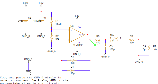
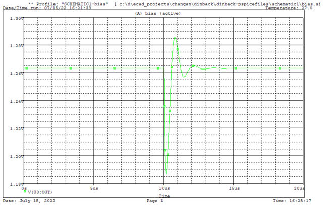
    I try to do the simulation like this, and still the glitch exists. I wonder in which way we could reduce the glitch as much as possible.

    R6/C4/R7 is used to simulate the ADC.

  • Hi,

    the standard way is to use a suited charge bucket filter (R5 and C3). Provided the ADC does not sample too often per second and the OPAmp is fast enough to make the charge buckte filter fully settle between the samplings, C3 can be increased. For a 10bit ADC with its 1024 steps, for instance, make C3 at least 2000 times bigger than C4.

    What is your ADC? And how often do you want to sample per seond?

    Kai

  • Hello

    The ADC is embedded in STM32U585, a SAR ADC, the sampling rate is 2000SPS. a 14 bit ADC

    Thanks!

  • Then increase C3 to 100nF.

    Kai

  • Hello

    Thanks for the recommendation. I wonder why this kind of thing do not happen when I use amplifier for a 50Hz signal. Very often, I use the amplifier for a 50Hz signal and followed by an ADC with roughly 2kSPS. But I never see a glitch from the ADC raw data.

    Thanks!

  • Why do you expect to see the glitch from the ADC raw data? If the OPAmp does not fully settle within the aquisition period of ADC, you simply take a wrong sample. To see the glitch you would need to sample the glitch every 100ns with a second much faster ADC in parallel to the first ADC causing the sampling glitch, which would make no sense at all.

    Kai

  • I don't expect to see the glitch, I just wondering how to make sure it could not be seen in AC signal.

    Thanks!

  • With the same OPAmp circuit, the same charge kickback filter and the same ADC you will always see the same glitch, independently of the signal to be converted. The glitch will always be superimposed to the input signal of ADC.

    When you take another ADC the glitch may disappear, especially if the ADC has an additional input buffer, by itself driving the sampling stage of ADC with the switched capacitor.

    And when you take another charge kickback filter the glitch may also disappear or at least change its shape. The bigger you make C3 in your circuit, for instance, the smaller the glitch will become, because C3 will more and more drive the switched capacitor at the input of ADC instead of the OPAmp. That's why C3 should be increased in your application.

    And when you take a much faster OPAmp the glitch may also become much smaller or at least much shorter so that the output of OPAmp can fully settle within the aquisition period of ADC.

    Kai