This thread has been locked.

If you have a related question, please click the "Ask a related question" button in the top right corner. The newly created question will be automatically linked to this question.

TLV3502-Q1: The window comparator circuit block is giving voltage dips at input as well as at the output during hysteresis region

Part Number: TLV3502-Q1
Other Parts Discussed in Thread: TLV3502, TL431, OPA2863

Hi,

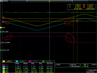
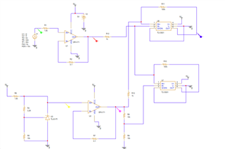
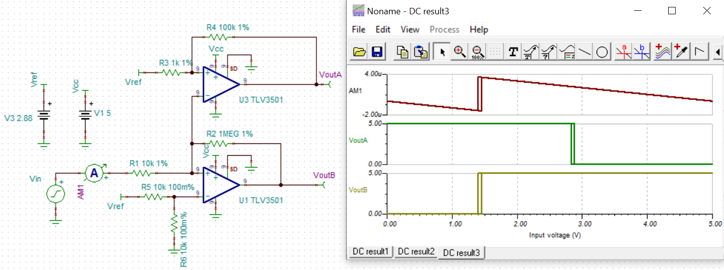
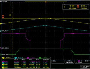
I am facing a issue, with TLV3502 comparator circuit block. When the high threshold comparator latches the output to 0 logic and high logic I get voltage dips at U31 buffer output as well as the comparator U32 output.

I don't face the same issue during lower comparator latching but the comparator U33 output also has a delay to reach final voltage. 

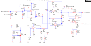
I changed the value of R479 and R485 from 1K to 22K, similarly R488 and R489 from 100K to 316K. The dips went away but my circuit latching threshold changed. I dont know why as my threshold from DB1 TL431 (left down corner) resistors or low threshold resistors were not changed. In simulation everything is working fine.

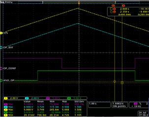
After changing the resistor values.

Please help me to resolve the issue. 

  • Rajat

    Thanks for your post and sorry I was not able to totally resolve your issue today.  I will work on this Monday and get back to you by Tuesday.

    In the meantime, from what you have described, I am not surprised that increasing the values of the resistors you mentioned impacted the dip of voltage since there is less current being fed back to your input.  You mentioned that simulation is still good but I am not sure exactly what you mean.  Are you saying your simulation shows same switching thresholds?  the math for scaling resistors in the feedback path is not so simple and I am wondering if you unintentionally altered your hysteresis and thus your switching thresholds.

    If you are using TINA, please upload your simulation file so we can use that as a starting point.

    Chuck

  • Hi Rajat,

    I see two issues:

    1. A resistor in the feedback loop of the fast OPA2863 wired as voltage follower is no good idea. This can cause stability issues. So either you reduce this resistor to zero or you add a phase lead capacitance to restore the phase margin again.

    2. I would add a RC filter between the outputs of OPA2863 and the resistors R479 and R485 to absorb the toggling noise coming from the outputs of comparators.

    Kai

  • Thanks Kai for your guidance.  I too saw the voltage follower with the resistor in the feedback.  I assume they have a reason for doing that but I agree, this is not ideal since the output will be stressed to keep up with the positive feedback of the comparator.  I still have not reviewed their change in resistors to see if this has an impact on the switching thresholds.  I will look into this further tomorrow.  

    Chuck

  • Hi Kai and Chuck,

    Thankyou for your response. 

    Before submitting simulation results and my tested results, i would like to share a few observations simply on TLV3502.

    1) Hysteresis more than 50mV is affecting the threshold latching points. The thresholds at which the TLV3502 is latching is due to the linear operation in hysteresis band. 

    2) The glitch that we are seeing above in the tested results is due to the hysteresis effect at the input (output of the buffer U34) hence the same glitch is observed at the output of comparator due to very low propagation delay.

    I see a solution to this, which I will implement and share the results.

    But I would like to know if the above observation points are making sense?

    Kai: The voltage follower needs to have a feedback resistor equivalent to input resistor to equate the input bias current at both inputs. But in this application it has helped to reduce the glitch/dip at buffer output.

    I will play with the circuit even more on testing part as the simulation is not working. 

    Regards,

  • Hi Rajat,

    Thanks for your post. It seems that the comparators are drawing too much current for your input source (your input buffer) and by increasing your resistors you were able to remove the output chatter. But, to keep your old hysteresis ranges, consider scaling up both the Input resistor (R479) and the feedback resistor (R489) in your circuit by the same amount (R479/R489 = 1/100).
    Here is a simulation with R479 = 10kOhm and R489 = 1MOhm. We can see that the hysteresis thresholds is the same while the current flow decreases:

    Previous Hysteresis Circuit:

    New Hysteresis Circuit:

    TI Tina Simulation File:

    Windowing_Hysteresis_Comparator_Circuit.TSC

    Thank you for your post,

    Rodrigo

  • Hi All,

    Increasing the resistance value and keeping the hysteresis 50mV has proven to remove the glitch or delay we are seeing above. One more point the testpoint wires added to the problem which has also been resolved now.

    Thanks.