This thread has been locked.

If you have a related question, please click the "Ask a related question" button in the top right corner. The newly created question will be automatically linked to this question.

LM231: Digital to analogue converter

Part Number: LM231
Other Parts Discussed in Thread: TINA-TI, OPA340, MAX660, TL7660, LM317, OPA2340, LM337

Hi Team,

I am a Diesel mechanic and while I have basic auto electrical and electronics understanding I don’t have the ability to design my own component in this instance and wondered if you may be able to help or point me in the right direction. I need a digital to analogue converter for a project I am currently working and need something that is assembled and programmed ready to connect, is this something you could provide? I understand you may need more information but I’ll do my best to describe what I am after. I am needing a DAC to convert the signal from 2 separate speed sensors form a 0.65v- 1.325 square wave digital signal to an analogue A/C sine wave signal that I have measured to be 5v peak to peak with the shaft speed at 190rpm and it needs to read between 0 and 1000 rpm. The pulse wheel on the shafts has 48 pulses per revolution. Obviously, the amplitude varies relative to speed of the shafts. The system voltage is 12 volts. I’d greatly appreciate any information you can provide.

Unfortunately I can't get any manufacturer data regarding the sensor or the module receiving the signal as such, only what I can measure. What this is is a Toyota rear axle that I am swapping out of a later model Toyota that has a much stronger final drive. The new axle has the digital 2 wire wheel speed sensors and the vehicle I am fitting it to requires the A/C signal, the signal is sent to the ABS module in the vehicle. Toyota don't supply any information on their equipment other than what is required to diagnose faults. I could as a last resort modify the axle to take the analogue wheel speed sensors and the pulse wheel to suit, however I'd like to avoid this if possible so as readily available part will still fit if required.

This is the only information I have regarding what the signal should look like, this comes from the diagnostic manual of the vehicle that I am upgrading the axle in.

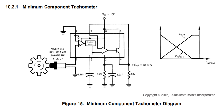
I wondered if this would work https://www.ti.com/lit/ds/snosbi2c/snosbi2c.pdf

Is it even possible to convert a digital speed signal to an analogue signal.

I don't think that if the amplitude of the analogue signal didn't vary with the change in frequency would be a problem.

Best Regards,
Tom

  • Hi Tom,

    if you want a frequency to voltage converter (F-V-converter), you could also take the LM2907.

    I am needing a DAC to convert the signal from 2 separate speed sensors form a 0.65v- 1.325 square wave digital signal to an analogue A/C sine wave signal

    This confuses me a bit. Do you also want to convert the square wave into a sine wave? Why would you want to do this? To make the F-V-converter properly work? This is not necessary. A F-V-converter usually needs a square wave at the input, no sine wave.

    Kai

  • Hi Tom,

    I agree with Kai. The LM2907 (or LM2917) Frequency to Voltage Converter (F-to-V) was primarily designed for automotive applications such as a tachometer input to voltage converter and would be the first, easiest applied device to consider.

    The datasheet has a number of different automotive F-to-V applications shown.

    https://www.ti.com/lit/ds/symlink/lm2907-n.pdf

    Regards, Thomas

    Precision Amplifiers Applications Engineering

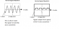
  •  I am not sure I have been clear in what I want to achieve, I hope this crude image will give more clarification. Kai the LM2907 you suggested looks to me like it is designed to receive a signal from an inductive type sensor where as I have a signal from a hall effect sensor generating a DC square wave high/low signal and I want to convert it to an A/C signal. 

  • Hi Tim,

    Indeed the LM2907 can be teamed up with a inductive sensor, but it can also be driven directly by an AC waveform such as a pulse train or square wave. The LM2907 charge pump comparator has the inverting input internally grounded and to trip the comparator the pulse train must go slightly below ground (0 V) for it to change state. Most often, a simple RC differentiator placed at the tach input with suffice in developing a negative/positive differentiated waveform that accomplishes the task.

    Alternately, the LM2917 does not have the comparator input grounded and is often biased a diode drop above ground (~ +0.7 V). Then, that voltage level is used for the comparator reference.

    Regards, Thomas

    Precision Amplifiers Applications Engineering

  • Hi Thomas thanks for your reply, would you be able to provide a schematic how the LM2917 would be interfaced into my basic 2 wire in and 2 wire out circuit and obviously power supply it also appears to need some external resistors. As I stated earlier this is not my speciality but I can follow basic electronic diagrams. 

  • Hi Tim,

    The LM2907 is very easily applied in the frequency (tach) to voltage configuration. The basic circuit shown below from the datasheet is a good example. The LM2907 is almost always applied with a single positive supply up to about +24 V. Therefore, the input signal and the output are ground referenced. Ground would be the other wire in your two-wire circuit.

    For you application the magnetic pick up would be replaced by a simple RC differentiator connected at pin 1. A series ~10 nF capacitor from your input pulse source to pin 1, and a 10 kilohm resistor from the pin to ground should take care of the differentiator. 

    Values R1, C1, and C2 are explained in the datasheet. Note that C1 is connected to pin 2, and R1 and C2 connect to pin 3. You can use the values see in the diagram below, or select them for a particular Vout, where Vout = fIN × VCC × R1 × C1. R1 is most often set to 100 kilohms.

    Regards, Thomas

    Precision Amplifiers Applications Engineering

  • Is someone able to help out with the values of C1, C2 & R1 please. 

  • Hi Tim,

    hmm, the longer I read your posts the more I get the feel that you may need something different. Is it that you want your Hall sensor signals look like coming from an inductive sensor? That you want to convert the positive square wave signals (sitting on a DC offset) coming from the Hall sensor into a true AC signal symmetrically swinging arround signal ground, preferably looking like a sine wave?

    Is it that you don't need a frequency to voltage converter? Is it that you don't need the LM231 or LM2907 at all?

    Kai

    PS.: Please note that I cannot decipher the second picture you posted. I mean the small picture with the sine wave and square wave.

  • Hi Tom,

    it needs to read between 0 and 1000 rpm. The pulse wheel on the shafts has 48 pulses per revolution. Obviously, the amplitude varies relative to speed of the shafts. The system voltage is 12 volts. I’d greatly appreciate any information you can provide.

    If I read your inquiry correctly, you may need to have digital counter reader, then convert it via ADC for the application. 

    In one of the example, you are getting 48 pulse/rev, and it combines with 0-1000 rpm, it will give provide 48 pulses/rev* 1000 rev/min or 48000 pulses/min, which is equivalent to 1000rpm. 

    If a circuit counts the number of continuous pulses over time, you will get rpm figure which is an average. Once you have the digital counter information per min, you can send the digital number to DAC + op amp buffer to get analog speed signal. 

    The F-to-V converter may work as well. This may be an alternative.

    Best,

    Raymond 

  • My sensor outputs a dc square wave signal that is around .6v when low and 1.3v when high. I want to make this signal into a alternating signal of the same frequency. 

  • Hi Tim,

    now it's clear what you are searching for Relaxed

    Some keywords in your original post like "DAC" and "LM231" were leading us on a completely wrong track...

    Kai

  • Hi Tim,

    I think you need a "Hall to VR converter" as discussed here:

    https://www.msextra.com/forums/viewtopic.php?t=75899

    Kai

  • Sorry for the misleading key words. 

  • Kai, thanks for the info. I am a little confused as to how the circuit in the post you shared the link to will be integrated into my circuit. Would you mind showing me how to connect this to my hall effect sensor please. 

  • Hi Tim,

    I haven't recommended this RC high pass filter. I just posted here the link of this discussion in the hope that you say: "Yes, that's what I need, a Hall to VR converter!" Relaxed

    Another hope was that you say: "Ok, I know where to buy such a Hall to VR converter!"

    I haven't recommended this RC high pass filter because it has several disadvantages:

    1. It needs about 3 x R1 x C1 = 3 x 1s = 3s to fully settle. See this simulation of a 100Hz square wave:

    tim_hall.TSC

    2. Even if you speed up the settling time by a factor of 1000, you will get another problem. At low frequencies the output signal is no longer a square wave (or at least very similar to a square wave) like with 1000Hz:

    but looks like this:

    The problem of this curve shape is that you don't have a fast traverse from the negative to the positive and vice versa. See the red circle:

    This is just not like a VR signal would behave. It's far away from a sine wave, even farer away than the square wave and can lead to mistriggering at lower frequencies.

    3. The RC high pass filter does not provide any gain. So if the input of your ABS module requires a higher input signal, then it may not trigger at any frequency, if the signal coming from the Hall sensor is too weak.

    Kai

  • Hi Tim,

    in my eyes the only remedy is to build (or buy) an active circuit comprising a comparator at the input with a threshold voltage of about 1.0V according to (0.65V + 1.325V) / 2 ~ 1.0V.

    If the comparator is supplied by a bipolar supply voltage of let's say +/-2.5V, then the output voltage of this comparator will show a square wave swinging between -2.5V and +2.5V resulting in a 5V peak to peak signal.

    And a simple RC low pass filter at the output of comparator will round a bit the edges of this square wave signal and provide some short-circuit protection.

    Kai

  • Hi Tim,

    There is an alternate device, the LM2917 that can directly utilize the sensor's square wave signal that is around 0.6v when low and 1.3v when high. The LM2907 required the input signal cross through 0 V and that is why I recommended the input differentiator. However, because the LM2917 charge pump input comparator does not have the inverting input grounded as the LM2907 does, that input can be biased above ground such as + 1 V. A voltage of +1 V lies about midway between the 0.6 V and 1.3 V your sensor outputs. 

    Shown below is an example of the LM2917N connected as a frequency to voltage converter. The ripple filter capacitor C2 has been set to 270 nF to a settled voltage at about 100 ms. Larger C1 values will reduce the ripple, but time to settle grows longer.

    The output voltage is about 850 mV for a 100 Hz, 0.6 V to 1.3 V square wave input. The following timing diagrams show how the output voltage VM1 moves higher with increasing frequency.

    I've attached the TINA-TI simulation file so you can try the model if you would like. Note that this LM2917N simulation model was not developed by TI, but rather by a brilliant person on the outside who had posted it to the web. Nonetheless, the model does a good job of simulating this V-to-F converter's functionality.

    If you think that a Hall Effect IC is more what you need TI does have such products, but they are not covered by this e2e forum.

    Regards, Thomas

    Precision Amplifiers Applications Engineering

    LM2917-14_V2F_01.TSC

  • Hi Kai thanks for your input and yes a hall to vr conversion is definitely what I am after, I need it to produce an alternating sine wave like an inductive speed sensor would produce. I apologise for my poor job of describing my requirements but as stated this is not my field. 

  • This does sound great but are you aware of such a circuit available to buy or even a diagram i could build. 

  • Hi Tim,

    I will draw a schematic for you. Give me a day...

    Kai

  • Hi Tim,

    Are you talking about Hall to Variable Reluctance (Vr) Sensor Adapter or Converter? Are there any AC signal amplitude requirements?

    Best,

    Raymond

  • Hi Tim,

    it took me a while to find a circuit which can be build with an OPAmp/comparator in a PDIP package Relaxed

    tim_opa340_1.TSC

    This circuit runs with a supply voltage of +/-2.5V. I will give you a schematic for the supply voltage generation later.

    What do we have?

    From the left comes the Hall signal voltage swinging between 0.65V and 1.325V. R5 and C2 provides a low pass filter removing noise from the signal line. The Hall signal is connected to the -input of OPAmp.

    The OPA340 is wired as a comparator. R6, R1 and R2 form a voltage divider and set a threshold voltage of about 1.0V at the +input of OPA340. To remove noise from the +2.5V supply voltage line R6 and C3 form a low pass filter. (This makes sense, when you will see the schematic of the supply voltage generation.)

    R3 forms a hysteresis and stabilizes the comparator by preventing mistriggering.

    R4 simulates the typical 1k source impedance of an inductive sensor. It also serves as a short-circuit protection and in combination with C1 as a low pass filter rounding the edges of the square wave output signal a bit.

    The output signal is a square wave with rounded edges swinging between -2.5V to +2.5V.

    For simplicity not shown in the schematic are two 100nF X7R decoupling caps which must be soldered directly (!) from each supply voltage pin of OPA340 to signal ground. "Directly" means with shortest connections.

    This is no ready circuit but only a first draft. It can be that C2, R3 and C1 have to be modified a bit. But this circuit should be a good starting point.

    There's still one issue:

    I don't know your Hall sensor and I don't know what load it needs to generate a signal swinging between 0.65V and 1.325V. If it has a simple voltage output, then everyting should be fine. But if it outputs a current and needs a shunt to develop this voltage drop, then we need to add such a shunt to the circuit. Can you give some details on the Hall sensor?

    Another issue is, that the input signal and output signal are not in phase. So an additional signal inverter might be necessary.

    The supply voltage generation uses a LM317 to produce +2.5V from the available +12V. And a TL7660 or MAX660 is used to generate the -2.5V from the +2.5V. The TL7660 (or MAX660) produces some unwanted switching noise at its input and output which must be suppressed by the help of some low pass filtering. This explains the need for R6 and C3.

    Kai

  • And here with the added signal inverter:

    tim_opa340_2.TSC

    You can then use the double OPAmp OPA2340.

    Kai

  • Kai, thank you for your help with the schematic. There are a couple of things I think may be an issue but probably are not difficult to fix with the knowledge you have.

    The signal that comes out of this circuit needs to provide both the positive and negative sides and show no continuity to the main vehicle ground as the inductive sensor produces the ac voltage within itself and the ABS module would detect a short to ground. The circuit also needs to simulate a 1.25k resistance of the old inductive sensor.

    The hall sensor is a 2 wire sensor and has a 10v supply to the positive side and a 140 ohm pull down resistor to ground to produce the square wave signal.

    Please forgive my lack of knowledge with complex schematics like this but the 2 yellow components, they are both listed on the drawing as OPAx340 but I assume by your description that they are different. You show 5 connections and they are not clear to me what is what of these connections, looking at the data sheet they have 6 connectors on them. The 100nF X7R decoupling caps you refer to, can you please identify where these should be installed in the circuit.

    Thank you greatly for your time and patients with me on this, i do appreciate it very much.

  • Hi Tim,

    I will answer your questions tomorrow. In the meanwhile I show you the schematic of the supply voltage generation:

    Kai

  • Thank you Kai, I look forward to your reply.

  • Hi Tim,

    The signal that comes out of this circuit needs to provide both the positive and negative sides and show no continuity to the main vehicle ground as the inductive sensor produces the ac voltage within itself and the ABS module would detect a short to ground.

    Ok, in this case you need galvanic isolation. Your first picture says that you need an isolation resistance from each line to battery ground of more than 10k. I have to think about it...

    The circuit also needs to simulate a 1.25k resistance of the old inductive sensor.

    This can easily accomplished by changing R4 to 1.25k. Your first picture says that 0.65k to 1.8k would be ok.

    The hall sensor is a 2 wire sensor and has a 10v supply to the positive side and a 140 ohm pull down resistor to ground to produce the square wave signal.

    Ok, you need a 140R shunt resistance at the input of the circuit.

    Please forgive my lack of knowledge with complex schematics like this but the 2 yellow components, they are both listed on the drawing as OPAx340 but I assume by your description that they are different. You show 5 connections and they are not clear to me what is what of these connections, looking at the data sheet they have 6 connectors on them.

    When using two OPAmps the OPA2340 instead of OPA340 can be used. The following scheme can be seen in the datasheet of OPA2340:

    Each of the two OPAmps has a +input pin, a -input pin and an output pin. Both OPAmps share the same supply voltage pins V- = -2.5V and V+ = +2.5V.

    The 100nF X7R decoupling caps you refer to, can you please identify where these should be installed in the circuit.

    In your circuit you will need to have a signal ground (= 0V) made of thick wires (or even a solid ground plane in a professional circuit). Connect all the signal ground symbols to it. See the lower end of C2, e.g., or the lower end of the 220µF/50V cap. These symbols stand for "signal ground". Also the minus pole of car battery should be connected to signal ground. (But as you need galvanic isolation I have to make some changes...)

    The decoupling caps would be mounted with one terminal connected to the according supply voltage pin of OPA2340 and the other terminal connected to signal ground. Section 10.2 of datasheet of OPA2340 gives an example.

    Do you have a friend who is experienced in building up electronic circuits and could assist you?

    Ok, I have to think about the galvanic isolation issue and will come back later.

    Kai

  • Hi Kai, thank you so much for your help i appreciate it very much. 

    I have connected with a colleague who can build the circuit for me if you can provide an overall schematic I will pass it on and see how he goes with it. 

  • Hi Tim,

    I have connected with a colleague who can build the circuit for me if you can provide an overall schematic I will pass it on and see how he goes with it.

    That's good to hear.

    I would give this scheme a try:

    tim_opa340_5.TSC

    I will explain it later.

    Kai

  • Hi Tim,

    ok, you will need galvanic isolation. And this not only for the signal but also for the supply voltages.

    The HCPL-2211 is a nice optocoupler with good isolation, moderate speed and needing only a small LED current. This optocoupler is used for the isolation of signal. Everyting right of the optocoupler must be galvanically isolated from everything left of it.

    Also, the +5V supply voltage of the left side can be generated from the car battery. But the +/-2.5V supply voltages on the right side must be generated by an isolated supply, for instance by the help of a RECOM DC/DC-converter providing isolated outputs.

    To make things not too complicate I would suggest that you first test the circuit with the right side powered by simple batteries and not by the RECOM DC/DC-converter. If everything works properly, then we can build an isolated power supply by the help of this RECOM converter. The DC/DC-converter could be something like this:

    RxxPxx-1709900.pdf

    For the test version with the batteries I still have to draw a schematic for you which I will show later. It will contain the LM317 / LM337.

    Kai

  • Hi Tim,

    here comes the supply voltage generation:

    The +5V generation from the car battery can be used for the two sensors together. Spend each of them the OPA340 circuit ("U3") on the left side of HCPL-2211 including one HCPL-2211. Or by other words, for two sensors you need one LM7805, two OPA340 and two HCPL-2211 in total. Instead of the two OPA340 you can take the dual OPAmp OPA2340 for this.

    The right side of HCPL-2211 including the HCPL-2211 and the associated OPA340 circuit ("U1") are powered by the +/-2.5V supply. The inputs of LM317 and LM337 are supplied by two separate 7.5V batteries.

    For two sensors you will need two such +/-2.5V supplies. And to ensure galvanic isolation not only from the car battery and the MCU inputs but also from sensor to sensor, the two +/-2.5V supplies must be totally separated from each other. This means that you will need two LM317, two LM337 and four 7.5V batteries in total.

    To summarize, you will need one LM7805, one OPA2340 dual OPAmp, two HCPL-2211, two OPA340, two LM317, two LM337 and four entirely separated 7.5V batteries.

    For the 7.5V batteries five standard 1.5V AA alkaline batteries in series should do. Such an 1.5V AA alkaline battery has a capacity of more than 2000mAh and the circuit will not draw more than 20mA.

    Kai