This thread has been locked.

If you have a related question, please click the "Ask a related question" button in the top right corner. The newly created question will be automatically linked to this question.

TLV1701: Device keeps burning

Genius 15139 points
Part Number: TLV1701

Hi Experts,

Seeking your assistance on this query:

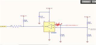
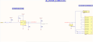
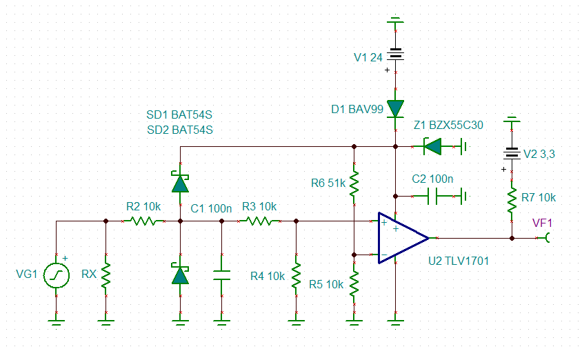
The part number in question is TLV170x - 2.2V to 36V microPower Comparator.
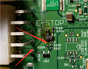
We're supplying the chip with 24V, using the comparator as an overvoltage sensor (Estop circuit).
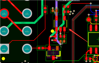
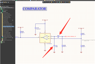
The chip keeps getting fried, and I'm speculating whether this could be related to the diode clamps connected to the supply rails, please see below.

Regards,
Archie A.

  • Hi Archie,

    Sorry you're running into this issue. Just a few questions:

    1) Whats the voltage on the IN+ pin? How large is it going? If it is going above VCC + 0.5V, it will be violating the abs max rating.

    2) Can you confirm on the board that voltages are what you expect? ie, is the chip actually being powered by 24V? Are the input pin voltages within the common mode voltage range? 

    3) If you replace the device with another sample, do you run into the same issue?

    4) Can you share PCB layout? 

    -Chi

  • Hello Chi,

    Thanks for responding. Cx responded:

    1) Whats the voltage on the IN+ pin? How large is it going? If it is going above VCC + 0.5V, it will be violating the abs max rating.

    15V at all times until the Estop button is pressed. Once the Emergency stop button is pressed, the voltage should fall below the 12V reference and the comparator should have a low output. IN+ should not go over 24V ideally.

    2) Can you confirm on the board that voltages are what you expect? ie, is the chip actually being powered by 24V? Are the input pin voltages within the common mode voltage range? 

    Yes, the voltage values are accurate and there are no spikes that could damage the comparators. I'm planning to thicken the copper traces around the E-STOP circuit to make sure they can handle the current / voltage. Maybe that's the issue? But still shouldn't burn the chip.

    3) If you replace the device with another sample, do you run into the same issue?

    Yes, we have multiple boards in the field with the same problem.

    4) Can you share PCB layout? 

    I'm attaching the entire ESTOP circuit layout part of the PCB board.

    Thank you.

    Regards,
    Archie A.

  • Hi Archie,

    Thanks for the follow up. What is the use of R339? Can you use a current limiting series resistor instead? Other than that, I don't really see any issues with your schematic which makes me think its possibly something from the layout if you consistently see the issue from multiple samples. The image you sent only shows the schematic, can you send the actual board layout with traces? Have you tested this circuit through prototyping/breadboarding? If not, can you?

    Is there a case where the input is applied before the device is powered on? When does the chip actually get fried? 

  • Hi Archie,

    I don't understand the "ESTOP". I don't see any signal voltage. Can you give some details?

    Also, if the input signal of comparator is leaving the board to the outer world, wouldn't it be a good idea to add some protection against ESD, EFT (burst), surge, overvoltages or even inductive kickback? The comparator appears to me to be entirely naked and unprotected.

    Kai

  • Thanks Chi and Kai,

    We'll send the PCB layout as soon as it would be available, waiting on Altium license renewal as per client.

    Mainly, R339 is a pull down resistor, not sure why the previous engineer added that there. 

    Question from Cx:
    It looks like the problem could definitely be on the layout, or maybe due to negative voltage on the output, so maybe add a diode at the output as well?

    Regards,
    Archie A.

  • Hello ArTzy,

    Please provide a complete schematic, including the output load (just a processor?) and the source of the 15V for the EStop loop.

    Does the EStop button open the loop? Or ground the loop?

    When does it fail? When the button is pushed? Released? A power-up/down?

    Are there any inductive loads (relays, solenoids, buzzers) on the 15V or 24V supply? Do they have diode EMF supressors?

    Does the 24V drop out before the 15V? That would DEFINITELY cause some damage (back feeding the entire 24V supply from the 15V supply through the ESD diodes). If this is the case, then a series resistor on the positive input (as shown scribbled in red) is a must to limit the current. It would also be good to add a diode in series with the comparator power to prevent backfeeding the supplies.

    Destruction like that does not randomly happen. That is a severe overstress (to put it mildly) - either over-current or a latch. Damage such as that takes many watts of power.

    Yes, R339 is a pull-down resistor to ensure that the output goes to GND if the ESTOP connection is opened. It is essential for proper operation.

    Is it possible to get a scope shot of the circuit when the button is pushed and during power up/down? Showing IN+, IN-, V+ and OUT. That will tell us a lot.

    Feeding an input directly from a supply, especially from a separate supply, is not recommend without adding a current limiting resistance in case of sequencing issues or transients.

  • Hi Paul,

    Attaching some quick snapshots of the comparator layout on the PCB board:

    Let me know if additional information needed.

    Thank you.

    Regards,
    Archie A.

  • Yes, a complete schematic...

    Kai

  • Hi Artzy, 

    Thanks for the layout. We are still waiting for your complete schematic. Whats on the output? Answers to Paul's questions would help guide us to see what the issue is.

    Have you tested this circuit through prototyping/breadboarding? 

    Is there a case where the input is applied before the device is powered on? When does the chip actually get fried? Can you show scope shots of your inputs, outputs, and supplies?

  • Hello Experts,

    Refer to the responses below.

    Can you provide a complete schematic, including the output load (just a processor?) and the source of the 15V for the EStop loop.
    ​I'm attaching a quick powerpoint that explains how the ESTOP circuit operates across our entire setup. The source of the 15V is coming from the power cabinet (PCS). The voltage line stretches across all dispensers through Molex connectors and meets the IN+ at the comparator. I can't share the full schematic unfortunately.
    Does the EStop button open the loop? Or ground the loop?
    ​Opens the loop.
    When does it fail? When is the button pushed? Released? A power-up/down?
    ​Ideally, the button is pushed in an emergency situation to immediately stop a charge session.
    Are there any inductive loads (relays, solenoids, buzzers) on the 15V or 24V supply? Do they have diode EMF suppressors?
    Don't believe they do.
    Does the 24V drop out before the 15V? That would DEFINITELY cause some damage (back feeding the entire 24V supply from the 15V supply through the ESD diodes). If this is the case, then a series resistor on the positive input (as shown scribbled in red) is a must to limit the current. It would also be good to add a diode in series with the comparator power to prevent backfeeding the supplies.
    Indeed, the 24V does drop out before the 15V, and that was actually our first speculation as per the datasheet: 
     
    Input pins are diode-clamped to the power-supply rails. Input signals that can swing more than 0.5 V beyond the supply rails must be current limited to 10 mA or less.
    ​Agree with you on that, I'll add a 10K in series on the positive input and possibly a 100nF cap to ground to filter out any noise coming from the 15V line. 
    ​Where do you recommend placing the diode exactly? 
    Destruction like that does not randomly happen. That is a severe overstress (to put it mildly) - either over-current or a latch. Damage such as that takes many watts of power.
    ​On the board layout, I also noticed that both the 24V line and 15V sense are traced on layers 4 and 5 respetively (purple and green), directly under the comparator, which could be adding to the problem. I will be moving them further away from directly below the chip. See picture below. 
    Yes, R339 is a pull-down resistor to ensure that the output goes to GND if the ESTOP connection is opened. It is essential for proper operation.
    ​Agreed.
    Feeding an input directly from a supply, especially from a separate supply, is not recommended without adding a current limiting resistance in case of sequencing issues or transients.

    Let me know if you need any additional information, I think I have a solid path forward. 
    Thanks again for your guidance.
    Regards,
    Archie A.
  • Hello ArtZy,

    I think the dropping of the 24V before the 15V is causing the problem. This does not seem to be a layout problem.

    If opening the loop causes the 24V to drop while the button is pushed, then when the button re-closes the 15V is again applied directly to the un-powered comparator input, and the ESD diodes are now back-feeding the entire 24V supply through the input ESD diodes - thus causing the magic smoke release. Essentially, the little ESD didoes are diode-OR'ing the 15V supply into the 24V supply.

    Along with the resistor, I would also place a diode in series with the comparator supply (pin 5) to prevent the back-feeding of the 24V supply. Between the SP_VDD_24V bus and the bypass capacitor. This also has the advantage of blocking any reverse supply transients..

    Any chance you can run the comparator on the 15V??

     I would try adding the resistor and see what happens. You can probably breadboard (kluge) on the existing board by removing R339 and externally adding the R339 and series R500 resistors at the loop input using 10k thru-hole resistors. That will at least show if this is the root problem.

    If it still blows up, then it's time to grab the scope and look for transients on the supply and input lines.

  • Hi Archie,

    I would do it as shown below:

    Signals entering the board from outside can be contaminated with all sorts of overvoltages (inductive kickback, for instance), EMI and noise. In these situations a low pass filter provided by R2 and C1 can be very helpful. The Schottky diodes SD1 and SD2 additionally clamp overvoltages to the supply rails of comparator while R2 limits the current through these Schottky diodes. R3 and R4 divide down the clamped input voltage by a factor of 2 in order to furtherly reduce the overvoltages arriving at the +input of comparator. The maximum voltage drop of BAT54S at 10mA is 400mV, limiting the overvoltage at the +input of comparator to <200mV which is considered to be a very safe value. D1 prevents any reverse current from flowing into the 24V supply when the comparator is powered down and a signal enters the circuit via R2. Z1 limits the supply voltage to a safe value then.

    archie_tlv1701.TSC

    Yes, it's true that the TLV1701 contains protection diodes at the inputs. But biasing them in the case of overvoltage will allow to develop input voltages exceeding the supply voltage of chip. This can result in latch-up or lock-up during power-up. It heavily depends on the chip whether this can happen or not. In older chips one remedy against latch-up was to decrease the current flowing through these internal protection diodes to very small values by providing an external diode clamp and adding a current limiting resistor between the external protection diode clamp and the internal protection diodes, as shown above. By this, the overvoltage current is almost entirely shunted arround the chip.

    RX plays the following role: If the stop signal runs throuhg relay contacts, it should be kept in mind that relay contacts need a minimum contact current to make a reliable turn-on. If the current through R2, R3 and R4 is too small, RX can be used to increase this current to a safe value.

    Mounting an additional ESD TVS at the input of the circuit (U62) is a very good idea. But this will only work when the ESD current can leave the board again without entering the circuit. This can be accomplished

    1. when the TVS sits directly at the socket pins, and

    2. when a 1...10nF Y-cap is mounted from the ground terminal of TVS to the metall chassis.

    Omitting the Y-cap can make things worse, because then the ESD is directly injected into signal ground and may run over the whole board in the hope to find a signal path to earth (directly or via stray capacitance !).

    For the same reason all signals entering or leaving the board should do this at only one edge of the board.

    Kai

  • Thanks Kai for the wonderful and thorough explanation :) 

    Archie,

    Let us know if you need any further help. I will close this thread for now. 

  • Hi experts,

    Thank you for all your fdetailed inputs here.

    Completely agree with the low pass filter, we've already added an RC filter on the schematic for the next board revision. 

    With regards to R3 and R4, we imagine that would be used if we'd like to bring the Voltage at IN+ below 15V correct? 
    I've been thinking about adding a zener clamp as well to act as a voltage reference, do you think that would be necessary?
    We imagine it would be similar to your D1 and D2.

    Thank you.

    Regards,
    Archie A.

  • Hi Archie,

    the zener diode cannot prevent the input voltage from exceeding the supply voltage like the Schottky diode clamp can:

    Kai

  • Artzy,

     The Schottky diode will allow you to clamp down the voltage when you go overvoltage since it is unidirectional and has a lower forward voltage.

    -Chi