This thread has been locked.

If you have a related question, please click the "Ask a related question" button in the top right corner. The newly created question will be automatically linked to this question.

PGA308: How to change the CFG2 to 0XDC0

Part Number: PGA308

Hi team,

One of my customers is evaluating PGA308 on their own board.
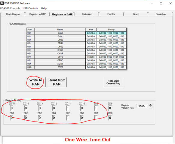
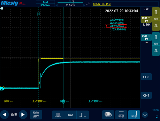
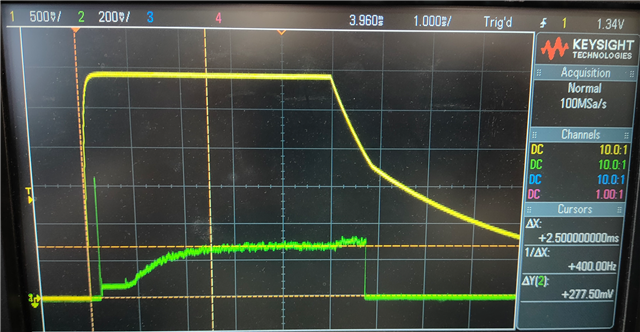
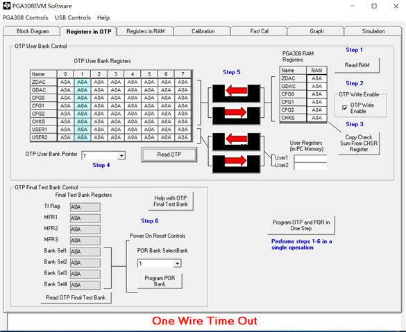
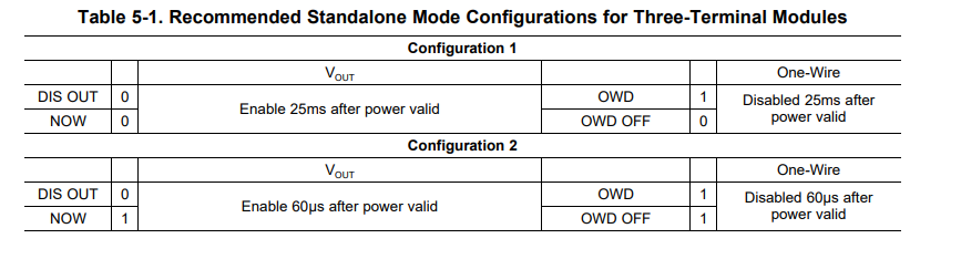
My customer changed CFG2 to 0XDC0 by first modifying the register in the Register bit, after clicking Write to RAM. But my customer doesn't know if that's correct, and what the next steps are? Could you help me to solve this problem? You reply would be much appreciated.

  • Hi Yang,

    I need additional information to be able to answer your question and/or debug the problem.

    1)  Can you please explain: is this a 3-wire, or 4-wire voltage output module? or a current output module?  

    2)  Kindly confirm the USB-DAQ jumper settings are in the correct configuration as shown below:

    3)  Please provide a complete schematic of the Custom PGA308 board including the supply connections, and bridge sensor connections. What is the bridge excitation supply used in this application.  Please show the bridge sensor excitation connections VEXC(+), VEXC(-) on your schematic.  Is the bridge sensor referred to the same GND potential. 

    4)  Please provide a diagram of the connections of the USB-DAQ to the Custom PGA308 sensor.  

    • GND connections: Please ensure that the PGA308 custom board and USB-DAQ are referred to the same GND potential.  If you intend to connect this custom board directly to the USB-DAQ controller, please ensure to connect your custom board GND to USB-DAQ J3, pin 21 (GND).  If you plan to use the PGA308EVM test board, you may connect to any of the GND1, GND2, GND3 test points.
    • 1-W connection: The 1-W connects to JMP7 pin2 of the PGA308EVM. Alternatively, you could connect to USB-DAQ controller J3, PIN11.  Ensure the PGA308 device on the PGA308EVM is not shorted to the same 1-W connection as the custom board (or remove the PGA308 device on the PGA308EVM board).
    • VOUT connection: The VOUT connects to VOUT_F test point of the PGA308EVM. Ensure the PGA308 device on the PGA308EVM is not shorted to the same Vout connection (you could remove R20 on the PGA308EVM board).  Alternatively, you could connect the output of your sensor to the USB-DAQ controller J3, pin 5. 

    5)  Can you please clarify the desired values on the CFG2 register in this application? Did you mean 0xDC0X on the post above?  The CFG register is a 16-bit word, the post above shows only 12-bit contents.

    6) Has the PGA308 device OTPs previously programmed on this device?  The GUI capture shows a warning where the One Wire has Timed Out.  This could be due to a fault in the connection on the one-wire interface; or due to previous OWD bit settings programmed in the OTPs.   Please keep in mind, it is important to access the One-wire while the interface is active.  Depending on the standalone configuration and how the OTPs have been programmed in the past, and the programmed OWD register settings, the one-wire may time out shortly after power-up.  Read in detail section 5.5 'Standalone Mode' and 'software lock mode', and refer to the details of figure 5-10 standalone algorithm on the PGA308 User Guide.

    Thank you and Regards,

    Luis

  • Hi Luis,

    Thanks for your kindly support. Below is the additional information about the problem.

    1)This a 4-wire voltage output module.

    2)  The customer has confirmed the USB-DAQ jumper settings are in the correct configuration.

    3)  This is the complete schematic of the Custom PGA308 board including the supply connections, and bridge sensor connections. And the diagram of the connections of the USB-DAQ to the Custom PGA308 sensor.  

    4)The product is 2.9V for normal customer use and is calibrated using the power supplied by the EVM board to output 0.5~4.5V between zero full and then proportional to the customer desired voltage range 0.29~2.61V signal.

    5)The desired value on CFG2 is the customer finds an issue: The customer requires that the power-on signal settles to output time of 2.5ms, but when actually measuring it, the data is still creepage at 2.5ms. The power-on time tested is as follows:

    When asked, the power-up time can be increased by changing register CFG2 to 0xDC00, but as follows, the chip will lock data to read and write, all output as A0A.

     Below is the customer calibration details.

    PGA308标定步骤.docx

    Thank you and Regards.

  • HI Enhui,

    Thank you for the detailed information.  I am out of office during the US Thanksgiving Holiday, and expect to be in office on Tuesday US time.

    I will review the information and expect to get back with an update by Tuesday US time.

    Thank you and Kind Regards,

    Luis

  • HI Enhui,

    Please clarify question (6), which is not answered above, has the PGA308 four-terminal module been previously programmed with OTP CFG2 0xDC00?

    When setting CFG2 = 0xDC00, the OWD bit is set to ‘1’ (Disable One-Wire) and OWD OFF bit is set ‘1’ (Disable One-Wire Instantly).    In this configuration, the OWD and OWD OFF bits disable the One-Wire Interface almost instantly, 60µs after power valid, locking out the device after Power-On-Reset.  As shown on table 5-1 on p67 of the PGA308 User’s Guide, Configuration 2 is only recommended for three-terminal modules that are programmed to the desired final values, once the User has ensure to have the correct calibration settings.  This is done to protect the OTP programmed values, but will make the re-programming of the PGA308 device OTPs difficult. 

    If the Customer has not decided on the PGA308 calibration final values, and is still experimenting with the calibration procedure, or wishes flexibility to re-program the OTPs, the alternative is to set OWD bit = ‘0’ to ensure easy access to the One-Wire.  Another alternative is to use Configuration 1 as shown on Table 5-1, p67 above, where the OWD bit is set to ‘1’ to disable One-Wire and OWD OFF bit is set ‘0’, allowing a 25ms typical delay after power valid before the One-wire interface is disabled.  

    As you have mention, in the hardware, the power-supply is still ramping-up before 2.5ms, and it is going to be a challenge to accurately control the timing of the power supply slew-rate, and sync the communication with the digital interface.  The hardware bypass capacitors, Ferrite L1, and any additional inductance/resistance through the hardware power supply connections will slow-down the supply slew-rate.

    If the device OTPs has been previously programmed to disable the one-wire, locking the device, you could re-populate the module with a fresh PGA308 unit, and set OWD bit to ‘0’ on the initial evaluation, and only set OWD bit to ‘1’, until the modules are programmed to final values.  The OTP User Bank X selection may be only set four times by programming the BANK SELx registers in order (where x = 1, 2, 3, or 4).

    Thank you and Regards,

    Luis