This thread has been locked.

If you have a related question, please click the "Ask a related question" button in the top right corner. The newly created question will be automatically linked to this question.

THS3001: THS3001 Gain Calculation

Part Number: THS3001
Other Parts Discussed in Thread: THS3491, TINA-TI

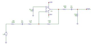
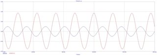
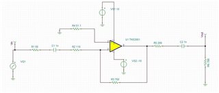
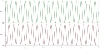
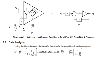
Hi. I needed some help calculating the gain using the THS3001 current feedback amplifier. I've looked at the application note SLOA019 that describes gain block analysis, but I am unable to determine what the transimpedance value (Zt) is based on the datasheet.

Also, I believe the analysis in the application note describes how to calculate the gain in terms of voltage. I am using the amplifier as a power gain block stage and I would like to understand how to calculate the gain in terms of power for different input and output impedances. I've tried creating the equivalent circuit diagrams and analyzing it that way, but my measurements don't match my calculations. Does anyone have suggestions on how to properly calculate this?

Thank you in advance.

  • You should use the THS3491 as a more modern device, also, can you attach your sim or bench circuit. Are you using a balun at the input by any chance?

  • Thank you for the response. Unfortunately, the THS3001 is already in the design so an alternative is not an option. No there is not a balun at the input. I've attached a simulation with the output results. The input impedance is 50Ω.

  • Hi Rishi,

    and the TINA-TI simulation is giving wrong results?

    Kai

  • I have not used TINA before, but I downloaded it today and gave it a try. It looks like it is giving me the same results as the previous simulation. Please see attached. I tried using the formula in the application note (I attached a picture as well), but I am not sure what the Zt value is.

    It seems like the voltage gain is just G = Rf / Rin, which is 4.7. Then there is a voltage divider at the output that brings it down to 3.6Vp. If I were to translate this to power, the simulation shows we have 6.3mW of peak input power and 19.6mW of peak output power. This would mean we have a power gain of 4.9dB (10*Log(19.6mW/6.3mW))? Is that right?

    I will try to capture some actual measurements to post, but in the meantime any ideas on how to calculate the voltage and power gain I am seeing in simulation? The formula differs from the application note. Also, the power gain changes from different loading conditions, right?

  • Hi Rishi,

    I think you take it way to complicated. Regarding to the gain setting feedback resistors a current feedback amplifier provides a voltage gain in an inverting amplifier circuit and non-inverting amplifier circuit exactly like a voltage feedback amplifier. It only works internally differently and because of bandwidth and stability issues you are not free to choose an arbitrary feedback resistance. For each gain the datasheet recommends an optimum feedback resistance. That's all.

    All the formulas you show have to do with the limitation due to a finite internal gain. The internal gain is called "open-loop transimpedance gain" ("ZOL") for the current feedback OPAmp and "open-loop voltage gain" ("AOL") for the voltage feedback OPAmp. I have not read your appnote completely but I'm pretty much sure that "ZOL" is your "Zt".

    The datasheet of THS3491 is better than the datasheet of THS3001 and shows a curve of "ZOL". See figure 22 of datasheet. You can clearly see that when you put this huge "ZOL" in the denominator of your formulas, the fractures heavily simplify. And, of course, the fracture "R1 / R2" is wrong and is a typo. It must be

    Vo / Vin = - R2 / R1.

    The datasheet of THS3001, on the other hand, shows a "transresistance curve" (see figure 9 of datasheet) which is "ZOL" at DC. And there is a curve in figure 30 from which the AC "ZOL" can be estimated.

    Kai

  • Thank you for the response and clarifying the differences between current and voltage amplifiers and the open loop parameters. Yes, the formula does simplify with a large Zt and I may be complicating this. For the circuit above, I calculate the gain as

    G = Rf/Rin

    G = (750/(110+50))

    G = 4.68

    I take the inverting input node as virtual ground. With a 1V input, the input current and input power is

    I_in = 1V/160Ω

    P_in = 6.25mW

    The output voltage is 4.68V. The output current and power is

    I_out = 4.68V/900Ω

    P_out = 24.3mW

    I then converted the power gains to logarithmic form

    5.89dB = 10*LOG (24.3mW/6.25mW)

    Does this seem right? The powers mentioned match the simulation results.

  • Hello Rishi,

      I do not see an issue with your calculations. I would also incorporate the feedback resistor into the calculation but would be a minimal value change.

    Thank you,

    Sima