This thread has been locked.

If you have a related question, please click the "Ask a related question" button in the top right corner. The newly created question will be automatically linked to this question.

TLV4171: Unused amps at single power supply

Part Number: TLV4171
Other Parts Discussed in Thread: LM358

Hi Team,

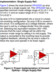
Customer's product uses TLV4171 by using single power supply and there have some unused amps.

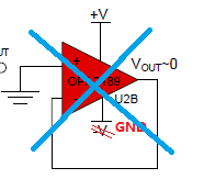
Based on TI tech notes, it doesn’t recommend to connect V+ to GND in single power supply, like:

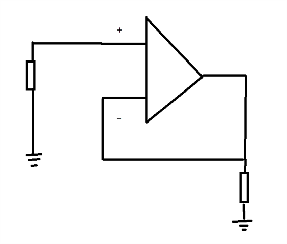
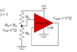
This circuit is properly implemented:

So why the first circuit is not recommended, even though the range of input voltage can be (V-)-0.1 to (V+)-2 in DS? Could you please provide your professional comments? Thanks.

By the way, what is the meaning of "(V-)" and "(V+)"? Is it refer to -2 < (V- + V+)/2 < -0.1? Thanks in advance.

BRs,

Francis

  • The input voltage is allowed, but the output voltage then is 0 V (eventually minus the offset voltage). This will overdrive the opamp and can increase the power consumption. (The voltage divider also uses power; consider using some voltage already available in your circuit.)

    V− and V+ are the (voltages at the) power supply pins. The parentheses are used to avoid confusion with nearby mathematical operators.

  • Hey Francis, 

    I agree with Clemens, we have the following TI Tech Note: How to Properly Configure Unused Operational Amplifiers

    All the best,
    Carolina 

  • I had read TLV4171 datasheet. It's an output rail-to-rail amplifier, while it input is not. In my opinion, there are two key point for amplifier not be used. One is power consumption,the other is signal not over input and output limit. So my experience tell me you could tie pins to ground with a small resistance, like pictures following. The value for resistance depend on Vos Ios and Icm. While in fact Hardware engineer won't calculate, they usually put a 1KΩ between ground and pin. 

  • you could tie pins to ground with a small resistance

    Such an input resistor would make sense for amplifiers like the LM358 that have PNP inputs. But for amplifiers with CMOS inputs, the input bias current is much smaller and might be positive (flowing into the input), so one resistor alone is not guaranteed to generate a useful voltage drop.

    (The resistor at the output is never needed and just wastes power.)

  • Hello Yin,

    The input resistor can help prevent damage if op amp ground differs from input ground. (poor layouts and with high current ground transients) 

    In my experience with OPAx171, supply current drops a small amount in non-linear operation. So this setup is unlikely to pose a problem, however it is not the most safe and most replaceable solution. What if in future the op amp is changed; would the new op amp also be good?

  • Hi Clemens,

    Why output resistor will waste power? Based on virtual break, it seems no current through this resistor, right?

    BRs,

    Francis

  • Yes, the current through it is similar to that of the input resistor, so it's negligible. It's just not needed.

  • Hi Clemens,

    Thank you. So what is the tiny difference between the output resistor and the input resistor? As I previously thought the output resistor just wastes power.

    just wastes power

    BRs,

    Francis

  • There can be reasons for the input resistor, but the output resistor does not help the circuit in any way.

  • Hi Minghao,

    the method Caro showed is perfect and I see no reason to experiment with any other circuit.

    I would choose the input voltage divider in such a way that the input voltage is within the common mode input voltage range of OPAmp and that the output voltage at the same time is within the linear output voltage range of OPAmp. Translated to the TLV4171 this means that input voltage should be within 0.35V and V+ - 2V, where V+ is the supply voltage of the single supplied TLV4171. So, for a supply voltage of +5V the input voltage should be within 0.35V and 3.0V.

    The proper biasing of unused OPAmps is important, because the four OPAmps in a quad package (or the two OPAmps in a dual package) may not be totally separated from each other. Sometimes the four OPAmps of a quad package share a common internal biasing circuitry and when one of the OPAmps is run outside its linear operating range, this may affect the performance of the three remaining OPAmps in the same package.

    By the way, in many circuits there's no need to add an extra voltage divider and the input of unused OPAmp can be connected to an already existing, suited DC potential.

    Kai

  • All,

    Thanks for all your help! No problem here.