This thread has been locked.

If you have a related question, please click the "Ask a related question" button in the top right corner. The newly created question will be automatically linked to this question.

INA210: INA210BIDCKR failed issue on pin4(IN+) and pin5(in-)

Part Number: INA210

Dear Support,

We are using the current-sense amplifiers INA210BIDCKR for output current monitor.

But it has some failed issue when working, analysis found that the pin4(IN+) and pin5(IN-) are shorted with GND.

In order to find the root cause, we catched some abnormal scope, and we cannot confirm if this scope can cause the IC broken.
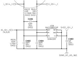
Our sample is two output 12V and paralled by oring, when only one 12Vo working, the INA210B of another circuit will generate leakage voltage, the scope are as follows,

Pin IN+ and IN- will slowly generate about 5V, pin V+ will generate about 1.8V, pin out will have 1.8V at sometime.
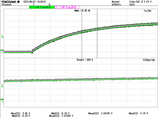
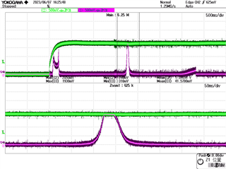
 

So we want to know if this leakage voltage will make IC broken, if not, what happened will cause the pin4(IN+) and pin5(IN-) shorted with GND?

Best regards,Felix

  • Hello Felix,

    I am looking at this and will respond shortly.

    Sincerely,

    Peter

  • Hey Felix,

    I will need a complete schematic showing how both INA210 are connected to the ORing diode, where the SVCC_12V_1 is sourced and returned, and how the grounds/returns paths of everything is connected.

    How many systems have you tested? How many show the abnormality?

    Does this INA210 work normally if the other 12V source is used? Even if it does work normally when its bus is ON, this does not mean it is not damaged.

    I am not convinced this is a damaged device yet. In order to prove this, please measure the differential voltage drop across R633 and and R631 with positive probe at the I_12V side and the negative probe at the INA210 input pin. I would like to see if the input bias current is out of specification, which would indicate a low-impedance path to ground within the device.

    The reason I am not sure if this is device damage yet is because this could be a simply result of the input bias currents having nowhere to go when the inputs are floating (because this 12V is not being used). Thus input pin voltage will float up to some point, which could cause the transient at OUT pin.

    The usual way to fix this issue is to place a pull-down resistance (~50k to 100kΩ) at input side at I_12V net. Although since the device is not being used it should not be necessary or practical to add this. However, you may want to remove this OUT disturbance, which would be fixed the same way with a weak pull-down resistance to ground.

    Sincerely,

    Peter

  • Thanks for your feedback.


    We have many kinds of GND in the schematic and it is not easy to sort out and explain to you.

    Although we catch the leakage voltage, this cannot convince that this will make IC damaged, I agree with you about this.


    So, we continue to catch other abnormal scope and it is as follow shown,


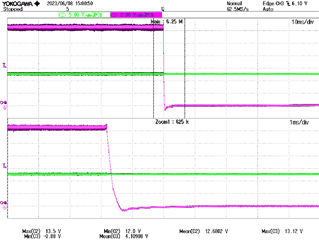
    When we shut down our module with full load, the IN+ pin will decrease from 12V to 0V, but from the scope, it will have a drop below 0V, the drop voltage is about -0.8V.


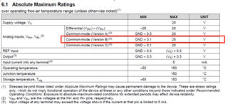
    In the datasheet, the allowable min voltage of IN+ pin is GND-0.1, so, we want to know if above-mentioned -0.8V will cause the IC damaged.


    Looking forward to your reply. Thank you

    Best regards,

    Felix

  • Hey Felix,

    The Vcm dropping to -0.8V is concerning and could absolutely be causing damage to the device. Please be sure when taking this measurement, that the scope's negative lead is connected close to or at the INA210 ground pin. This -0.8V drop could be tied to why I ask for how grounds are connected. If there is some inductance between INA210 GND pin and the load/12V source return, then a sudden voltage drop could cause an inductive kickback. You may want to examine the layout files and trace out how INA210 GND pin connects to the ultimate return path of the system and look for any point where impedance may rise. You could also test this out by physically connecting INA210 ground pin to source ground with a relatively heavy-gauge wire/cable and then repeat the power down at full load test.

    Please also try to answer my previous questions:

    How many systems have you tested? How many show the abnormality?

    Does this INA210 work normally if the other 12V source is used? Even if it does work normally when its bus is ON, this does not mean it is not damaged.

    In order to prove this, please measure the differential voltage drop across R633 and and R631 with positive probe at the I_12V side and the negative probe at the INA210 input pin. I would like to see if the input bias current is out of specification, which would indicate a low-impedance path to ground within the device.

    Sincerely,

    Peter